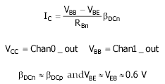
PC.6 SPICE Equations and Pin Diagram
PC.7 Measurement of the PNP Parameters
PC.8 DC Circuit Setup
PC.9 Measurement of the Amplifier Gain
Exercises and Analysis ExerciseC2.mcd - ProjectC2.mcd
|
SPICE Equation |
Description |
|
|
|
|
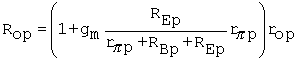
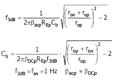
C.52 |
Amplifier gain. |
|
|
|
C.44 |
Base-collector gain. |
|
|
|
C.53 |
Amplifier load. |
|
|
|
C.40, C.41 |
NPN and PNP output resistance. |
|
|
|
C.47 |
Transistor output resistance. |
|
|
|
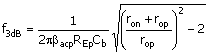
C.67 |
Design frequency of the amplifier. |
|
|
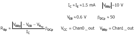
Components, PNP Calculate REp
Calculate RBp
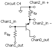
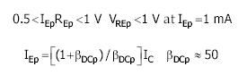
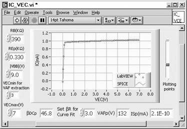
Procedure Circuit C4 is for obtaining the relevant SPICE parameters for the pnp. Of interest are VAFp, bDCp, and ISp. To obtain the parameters, connect Circuit C4 using the resistors calculated for this part (pnp). These will also be used in the complete amplifier. The VI for obtaining the parameters is IC_VEC.vi. Open IC_VEC.vi. Install, in their Digital Indicators, RBp and REp. Run the VI IC_VEC.vi with subVI IC_VECsub.vi open to observe the plot in progress. Reset VBB as necessary to obtain an active-region IC of about 1 mA. Verify that IC = 1 mA with |VBB|<10 V can be obtained. |VBB| should be roughly 10 V at IC = 1 mA for maximum measurement precision. Adjust parameter bR for a curve fit using VCEmax = 1 V. Note that VCEmin is automatically set to 0.5 V for small VCEmax.
Determine the value of VAF specifically for the range that includes
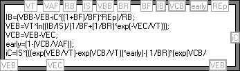
the bias value of VCE for the amplifier, which is VCE The computational subVI, SPICE_IV_Rep.vi, computes the SPICE plot, which is plotted along with the measured data. The Formula Node from the Diagram of SPICE_IV_REp.vi is shown below. A solution for IC as a function of VEC using the circuit and device equations is obtained. This is also explored in the project Mathcad file.
|
|
Components NPN RBp
If slightly different, use RBp > RBn. Design IC = 1mA.
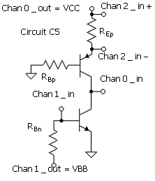
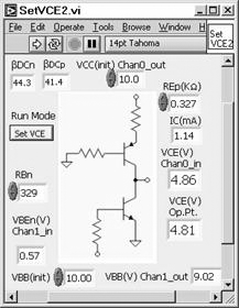
Procedure SetVCE2.vi ramps VBB downward from the maximum,VBB(init) = VCC(init). Thus, initially, the npn will be in saturation and VCE will be very approximately 100 mV. The first check is for one point, maximum VBB = VCC = 10 V. The initial goal is verify that the npn is in saturation and that the current is greater than 1 mA for VCC = 10 V. Connect Circuit C5. Note that the bottom of RBp is now ground and Chan1_out moves to the bottom of RBn. Also, the collectors are connected together and Chan1_in moves to the base of the npn. Move the plus side of Chan2_in and the top of REp to Chan0_out. Set in resistor values in SetVCE2.vi. Verify that VBB(init) = 10 V and VCC(init) = 10 V. Set the Run Mode switch to One VCC (logic 1). Run the VI. Verify that IC>1 mA and and that VCE is 50 to 300 mV (in saturation). SetVCE2.vi calculates the VCE operating point (bias voltage) as (VCC - VREp)/ 2 for any VCC (optimum signal swing magnitude). When the Run Mode is set to Set VCE, the execution of the VI halts when this level of VCE is reached.
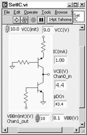
Set the Run Mode switch to Set VCE. Run the VI. Verify that the execution halts when VCE is about equal to VCE(V)Op.Pt. Note that in the example, IC = 1.14 mA for VCC = 10 V and VBB = 9.02 V. Verify that the final VCE is close to VCE(V)Op.Pt. Default the Front Panel to save the values of RBn and REp. SetIC.vi runs SetVCE2.vi as a subVI. It ramps VCC downward to find the VCC corresponding to the design IC = 1 mA. Open SetIC.vi and have SetVCE2.vi open as well. SetIC.vi will be a subVI in the gain measurement VI. Run the VI to verify that the VI can determine the VCC corresponding to IC = 1 mA. In the example, VCC has been ramped down to 9.0 V and VBB is now down to 8.1 V. The routine will occur automatically in the execution of the gain measurement VI.
|
|
Component Computation
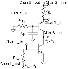
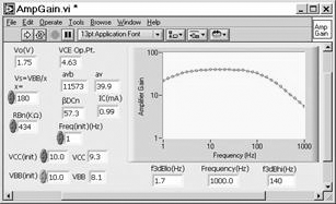
Procedure AmpGain.vi sweeps the signal frequency over the range finit<fs<1000 Hz. Note that on the low end of the sweep, this is a fairly slow process. The functiongenerator VI sends several cycles at each frequency, which is, e.g., 1 sec/ cycle at fs = 1 Hz. The amplifier voltage gain is calculated at each frequency step. This is the signal output voltage, Vo, divided by the signal input voltage, Vs. Vs is corrected for digital-to-analog error. The correction is performed by subVI, DAC.vi. The first measurement is made without Cb. Enter the value of RBn in the Front Panel of AmpGain.vi. Although it is defaulted in SetVCE2.vi, it is needed in the Top VI in the calculation of avb. Also open subVI's SetIC.vi and FG1Chan.vi to observe the program in progress. At least temporarily open SetVCE2.vi to verity that the component values in the Front Panel are correct and have been made the default values. Set Freq(init) to 10 Hz in the Front Panel of AmpGain.vi. Verify that VCC(init) and VBB(init) are set to 10 V. Run the VI. Upon completion of the execution there should be a low-frequency plateau in the response curve. The VI uses the maximum in the plot for the amplifier (circuit) gain. The roll-off at high frequencies is due to circuit board and transistor capacitance. Note that the example is with the capacitor in place. There will be no low-frequency roll-off without the capacitor. Now reset VCC(init) and VBB(init) to match the values in the Digital Indicators (in lieu of 10 V as in the example). The dc set up will be considerably faster. Re-run AmpGain.vi to verify that it functions properly.
If the gain curve appears already to be in the high-frequency roll-off at the lowest frequencies, re-run the VI with Freq(init) set to 1 Hz. Re-run the VI and adjust X (downward for increasing Vs) to obtain a Vo (signal sine-wave peak) of about 1 V or about one-third of VCE (operating point). Note that the DAQ limit must be set at 10 V to accommodate the dc + signal measured with Chan0_out. Therefore, the output signal voltage must be relatively large to have sufficient measurement resolution. Log the Front Panel. Add the capacitor, Cb, to Circuit C6. Set Freq(init) to 1 Hz. Run AmpGain.vi. If a proper selection of Cb was made, the response curve should have a flat portion as in the example. The flat segment contains the gain value. Note that if f3dBlo indicates 1 Hz, then it is less than 1 Hz. In this case, lower Freq(init) to obtain a curve that includes the f3dB frequency. It may be necessary to increase X (decrease Vs) for a satisfactory value of Vo, as the gain is higher with the capacitor. Log the Front Panel when a satisfactory result has been obtained. |
|