Microsistem cu RAM extern
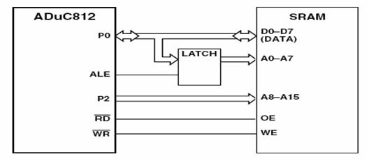
Se constata ca memoria RAM static (SRAM) este comandata cu semnalele /RD si /WR corespunzatoare citirii respectiv inscrierii informatiei. In cazul prezentat se considera ca magistrala de adrese este pe 16 biti(64 ko), partea superioara a adreselor fiind furnizata de portul P2 in timp ce partea inferioara a cuvantului de adresa este scoasa pe portul P0, multiplexata in timp cu datele.
Memorarea adresei inferioare se face in circuitul LATCH la aparitia semnalului de comanda ALE (Address Latch Enable).
Arhitectura tipica a unui uC
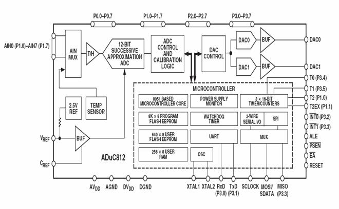
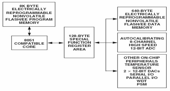
Acestea constau in UCP (CPU), o memorie program Flash care contine codul aplicatiei si o memorie Flash de date care permite inscriere per citire in timpul executiei programului. Microcontrollerul mai include de asemenea o memorie RAM (256 octeti).
Ca si circuite de interfata cu periferice pot fi identificate: un circuit CTC (3 Timer-Counter), UART si 2 interfete cu magistrale externe (SPI, I2C).
Functionarea microcontrollerului este determinata de un semnal de clock, generat cu un oscilator (cristal de cuart extern).
Structura mai include: un circuit pt. monitorizarea tensiunii de alimentare si un circuit Watchdog.
La elementele mentionate se mai adauga cele 4 porturi care asigura comunicatia cu exteriorul (P0, P1, P2 si P3).
OBS: Datorita tendintei de reducere a nr. de pini, liniile unora dintre porturi au functii multiple (Ex. tipic este portul P3)
In cazul acestui microcontroller pe acelasi cip sunt adaugate: un convertor analog-numeric cu 8 canale si 2 convertoare numeric-analogice (DAC0 & DAC1).
OBS: In situatile practice nu intervin toate elementele mentionate mai sus, dupa cum pot aparea alte elemente suplimentare fata de cele mentionate. Ex: magistrala CAN. De regula nu apar convertoarele analog-numerice si cele numeric-analogice (apar ca o exceptie).
Organizarea memoriei program
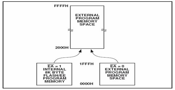
Microcontrolerele actuale au o memorie program pe cip, care acopera necesitatiile majoritatii aplicatilor. Cu toate acestea ele au prevazute posibilitatea conectarii in exterior a unei memorii program. Citirea memoriei program intern, respectiv a memoriei program externe este conditionata de nivelul logic aplicat pinului /EA (External Addressing).
Organizarea memoriei de date
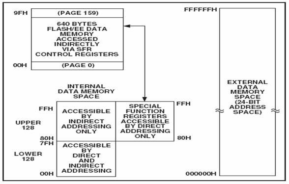
Similar cu cazul memoriei program exista posibilitatea utilizarii numai a unui RAM intern de mica capacitate, respectiv a RAM-ului intern impreuna cu un RAM extern de capacitate mai mare. Cu cateva exceptii instructiunile care manipuleaza date sunt cu referire la RAM-ul intern avand in vedere timpul redus de acces al acestuia.
Memoria RAM externa, daca exista, poate fi accesata cu instructiuni corespunzatoare acestui scop.
In unele situatii microcontrolerul include pe cip si o memorie Flash de date. Aceasta memorie poate fi accesata in timpul executiei programului spre deosebire de memoria Flash program, care este programata o singura data la realizarea aplicatiei.
Jumatatea superioara a memoriei RAM interna include doua zone: una cu adresare indirecta (utilizata ca memorie RAM interna obisnuita), precum si o zona cu adresare directa, numita zona SFR (Special Function Registers).
In aceasta ultima zona sunt plasati toti registrii prin care se programeaza functionarea dispozitivelor periferice, precum si registrii implicati in transferul de date realizate cu aceste dispozitive periferice.
Structura memoriei interne de date
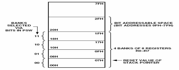
Din punct de vedere al programatorului prezinta interes jumatatea inferioara a RAM-ului intern.
Aceasta zona de memorie are o organizare speciala care include:
Modelul memoriei pentru programare
Include 111 instructiuni
Majoritatea sunt reprezentate in memoria calculatorului
pe 2 sau 3 octeti
Pentru programator, instructiunile sunt specificate prin
mnemonice, provenite din limba engleza si care sugereaza natura operatiei efectuateO instructiune include o mnemonica pentru operatie si de la 0 la 3 operanzi, separati prin virgule
Cu citeva exceeptii, instructiunile prelucreaza informatia
din memoria RAM interna a microcontrolerului
Destinatia este specificata prima si apoi sursa
Structura unui program
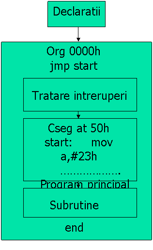
Structura unui program include mai multe blocuri specifice:
Sistemul de intreruperi
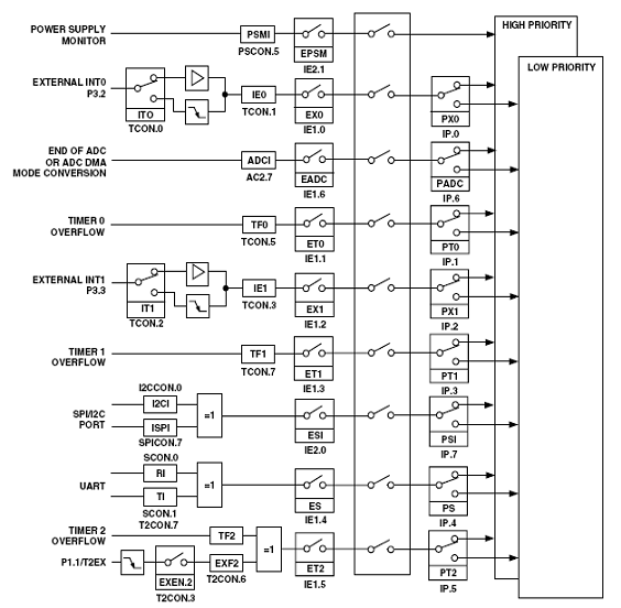
Aparitia unei cereri de intrerupere determina setarea bistabilului aferent. Stergerea bistabilului se face in unele situatii automat de catre UCP, iar in alte situatii trebuie facuta prin program. In orice caz stergerea bistabililor aferenti intreruperilor active pe nivel nu poate fi facuta numai dupa modificarea nivelului.
Portul paralel
Reprezinta o structura hardware interne microcontrolerului
care asigura schimbul de informatii digitale cu dispozitive
Externe,
Numarul de linii de port este egal cu numarul de biti
pe care este reprezentata informatia in microcontroler,
De regula un microcontroler are 4 porturi,
Liniile unui port pot fi programate sa functioneze ca iesiri
sau ca intrari,
Unele linii de port dot fi utilizate ca intrari pentru CAN,
De regula liniile unui port indeplinesc functii multiple.
Structura portului P0
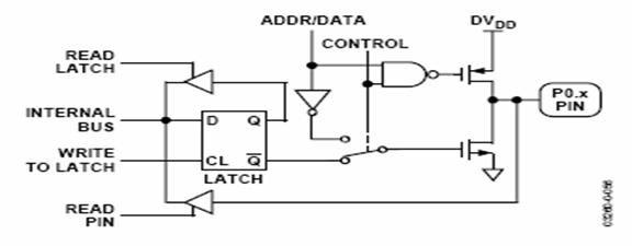
Portul P0 poate functiona ca un port paralel normal sau ca functie alternativa poate asigura transferul de date, respectiv octetul Low al adresei atunci cand se acceseaza o memorie externa (la executia unor instructiuni MOVX ).
La functionarea ca port se poate citi prin instructiuni corespunzatoare fie starea Latch-ului fie starea pinului. Pt ca pinul sa se comporte ca o intrare trebuie inscris "1" in Latch (Tranzistorul de jos - blocat). Daca linia de port e folosita ca iesire tranzistorul de sus este blocat si prin urmare linia se comporta ca o iesire de tipul "drena in gol".
In cazul functie alternative semnalul Control devine "1" si in consecinta tranzistorul de jos va fi comandat cu un bit de date/adresa. Acelasi bit comanda in mod coresp. si tranzistorul de sus, cele doua tranzistoare comportandu-se ca un etaj de iesire al unui inversor (conduc in contratimp). Utilizarea unei asemena scheme diferita fata de iesirea "drena in gol" asigura curentii de comanda relativ mari necesar pentru comanda magistralelor de date, respectiv de adresa.
Tranzistorul de sus este MOS cu canal indus de tip "p", iar cel de jos este canal indus de tip "n".
Structura portului P1
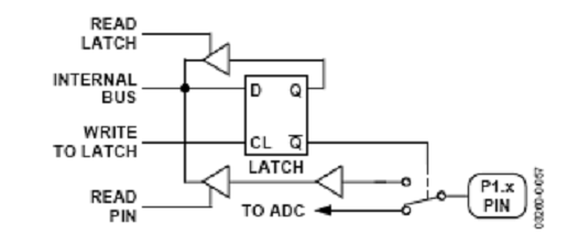
In cazul de fata linile portului P1 sunt utilizate si ca intrari la convertorul analog-numeric. Linile portului nu pot fi utilizte ca linii de iesire de aceasta data, starea bistabilului determinand ca pinul sa fie folosit ca intrare pt. convertorul analog-numeric, fie ca intrare numerica a portului.
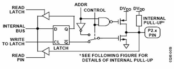
Structura portului P2
Structura portului P3
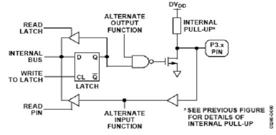
Se constata ca in cazul portului P3 circuitul de iesire nu este de tipul Push-pull, deoarece portul P3 nu este utilizat pentru comanda magistralelor. La fel ca si in situatile precedente pinii portului P3 accepta functii alternative (intrari ale numaratoarelor T0 si T1, intrari pentru intreruperi externe, etc.).
Functii multiple prin multiplexare in timp
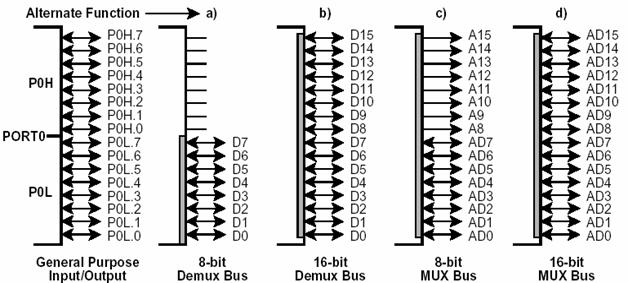
Figura de mai sus reflecta functiile multiple pe care le poate asigura portul P0 dintr-un microcontroler pe 16 biti. Pe langa functia de baza de intrari iesiri generale este posibila scoaterea pe magistrala a datelor reprezentate pe 8, respectiv 16 biti (modul nemultiplexat), precum si scoaterea pe magistrala multiplexate in timp a datelor si a adreselor (fig. c si d).
Circuitele de numarare/temporizare
Indeplinesc doua functii distincte:
Functia de numarare a unor evenimente externe,
Functia de generare a unor evenimente, la intervale de timp bine
precizate
Includ in mod obisnuit trei circuite de numarare/temporizare denumite T0, T1 si respectiv T2.
Circuitele T0 si T1, care functioneaza in mod asemanator, prezinta patru moduri de lucru (Mod 0, Mod1, Mod2 si Mod 3), in timp ce T2 are numai trei moduri de lucru.
Fiecare circuit de numarare/temporizare include doua registre (THx, TLx, x=o, 1 si 2) a caror functionalitate este programabila prin doi registri SFR (TMOD, TCON).
Modurile de lucru pentru T0 si T1
M1 M0
TH1 operates as an 8-bit timer/counter. TL1 serves as 5-bit prescaler.
16-Bit Timer/Counter. TH1 and TL1 are cascaded; there is no prescaler.
8-Bit Autoreload Timer/Counter. TH1 holds a value that is to be reloaded into TL1 each time it overflows.
Timer/Counter 1 stopped.
Modurile de lucru pentru T2
Functionare T0 in Modul 0
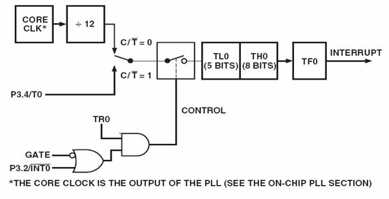
In modul 0, T0 functioneaza ca un numarator cu 8+5=13 biti dependent de starea bitului (C/nT) numaratorul poate functiona in regim de temporizator (cand se numara perioadele oscilatorului intern) sau in regim de numarator cand sunt numarate impulsurile aplicate la P3.4.
Intrarea P3.2 poate fi utilizata pentru a valida, respectiv invalida procesul de numarare in situatia in care se doreste masurarea duratei unor impulsuri (aplicate la intrarea P3.2).
Bitii TR0 si GATE pot fi programati fiind disponibili in registrele TMOD, TCON.
Functionare T0 in Modul 1
Modul 1 de functionare este similar modului 0 cu diferenta ca TLO functioneaza pe 8 biti (in loc de 5 biti).
Functionare T0 in Modul 2
In modul 2 de functionare TL0 functioneaza ca un numarator pe 8 biti in timp ce TH0 functioneaza ca un registru al carui continut poate fi modificat prin program si care este automat incarcat in TL0 ori de cate ori apare depasirea capacitatii acestui numarator. Modul 2 de lucru se recomanda a fi utilizat in situatia in care se doreste modificarea cu rezolutie ridicata a factorului de divizare pe care il realizeaza TL0.
Functionare T0 in Modul 3
Se constata ca in modul 3 TL0 functioneaza ca numarator/temporizator cu 8 biti utilizand toate celelalte resurse ale lui T0, iar TH0 este conectat exclusiv ca numarator-temporizator utilizand bistabilul de intreruperi a lui T1 aflat in stare inactiva
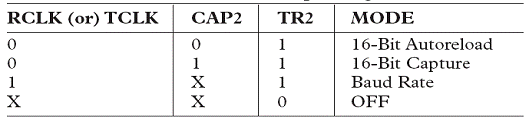
Functionare T2 in Modul 16 bit-Autoreload
Modul de lucru Autoreload a lui T2 este asemanator cu modului 3 de lucru de la T0 cu diferenta ca este incarcat continutul registrelor RCAP2L si RCAP2H, fie la aparitia unei depasiri a capacitatii de numarare, fie la aparitia unui front de cadere la intrarea T2EX. Totodata sunt basculati bistabilii TF2, respectiv EXF2, fapt ce conduce la generarea unei intreruperi.
Functionare T2 in Modul 16-Bit Capture
Modul de lucru 16 biti Capture este similar functionarii precedente cu diferenta ca de aceasta data la aparitia unui evenimet extern (front de cadere la T2EX) este captat continutului TL2 si TH2 in RCAP2L si RCAP2H.
Un asemenea regim de lucru este util in situatia in care trebuie masurate intervalele de timp intre evenimentele externe.
Functionarea sincrona
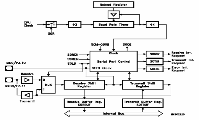
Synchronous mode supports half-duplex communication, basically for simple IO expansion via shift registers. Data is transmitted and received via pin RXD0/P3.11, while pin TXD0/P3.10 outputs the shift clock. These signals are alternate functions of Port 3 pins. Synchronous mode is selected with S0M='000B'.8 data bits are transmitted or received synchronous to a shift clock generated by the internal baud rate generator. The shift clock is only active as long as data bits are transmitted or received.
Synchronous transmission: begins within 4 state times after data has been loaded into S0TBUF,provided that S0R is set and S0REN='0' (half-duplex, no reception). Data transmission is double buffered. When the transmitter is idle, the transmit data loaded into S0TBUF is immediately moved to the transmit shift register thus freeing S0TBUF for the next data to be sent. This is indicated by the transmit buffer interrupt request flag S0TBIR being set. S0TBUF may now be loaded with the next data, while transmission of the previous one is still going on. The data bits are transmitted synchronous with the shift clock. After the bit time for the 8th data bit, both pins TXD0 and RXD0 will go high, the transmit interrupt request flag S0TIR is set, and serial data transmission stops.
Pin TXD0/P3.10 must be configured for alternate data output, ie. P3.10='1' and DP3.10='1', in order to provide the shift clock. Pin RXD0/P3.11 must also be configured for output (P3.11='1' and DP3.11='1') during transmission.
Synchronous reception is initiated by setting bit S0REN='1'. If bit S0R=1, the data applied at pin RXD0 are clocked into the receive shift register synchronous to the clock which is output at pin TXD0. After the 8th bit has been shifted in, the content of the receive shift register is transferred to the receive data buffer S0RBUF, the receive interrupt request flag S0RIR is set, the receiver enable bit S0REN is reset, and serial data reception stops. Pin TXD0/P3.10 must be configured for alternate data output, ie. P3.10='1' and DP3.10='1', in order to provide the shift clock. Pin RXD0/P3.11 must be configured as alternate data input (DP3.11='0').
Synchronous reception is stopped by clearing bit S0REN. A currently received byte is completed including the generation of the receive interrupt request and an error interrupt request, if appropriate. Writing to the transmit buffer register while a reception is in progress has no effect on reception and will not start a transmission.
If a previously received byte has not been read out of the receive buffer register at the time the reception of the next byte is complete, both the error interrupt request flag S0EIR and the overrun error status flag S0OE will be set, provided the overrun check has been enabled by bit S0OEN.
Asynchronous Operation
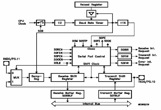
Asynchronous mode supports full-duplex communication, where both transmitter and receiver use the same data frame format and the same baud rate. Data is transmitted on pin TXD0/P3.10 and received on pin RXD0/P3.11. These signals are alternate functions of Port 3 pins.
Circuit pentru
modularea impulsurilor
in durata (PWM)
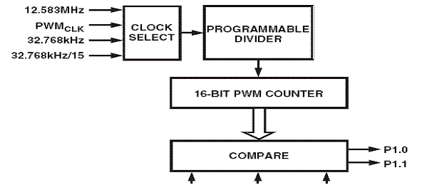
Utilizeaza un registru de comanda WMCO si inca patru registri SFR:PWM0H, PWM0L, PWM1H, and PWM1L.
Factorul de divizare:
CDIV1 CDIV0 Description
0 0 PWM Counter = Selected Clock/1
0 1 PWM Counter = Selected Clock 4
0 PWM Counter = Selected Clock/16
1 PWM Counter = Selected Clock/64
Selectia sursei impulsurilor de tact:
CSEL1 CSEL0 Description
0 PWM Clock = fXTAL/15
0 1 PWM Clock = fXTAL
1 0 PWM Clock = External Input at P3.4/T0/PWMCLK
1 1 PWM Clock = fVCO (12.58 MHz)
Regimurile de lucru
MD2 MD1 MD0 Mode
Mode 0: PWM Disabled
Mode 1: Single Variable Resolution PWM
Mode 2: Twin 8-bit PWM
Mode 3: Twin 16-bit PWM
Mode 4: Dual NRZ 16-bit DAC
Mode 5: Dual 8-bit PWM
Mode 6: Dual RZ 16-bit DAC
1 1 1 Reserved for Future Use
SPI Protocol (cont.)
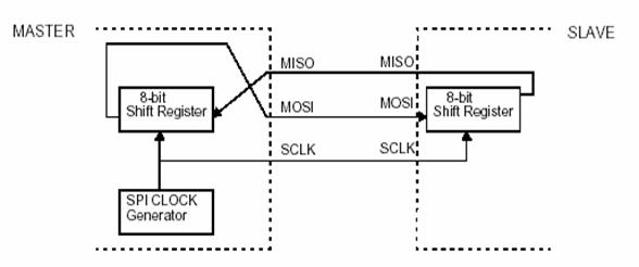
n Hardware realization is usually done with a simple shift register
n SPI interface defines only the communication lines and the clock edgeThere is no specified flow control! No acknowledgement mechanism to confirm receipt of data.
CAPCOM Unit Block Diagram
A CAPCOM unit is typically used to handle high speed IO tasks such as pulse and waveform generation, pulse width modulation, or recording of the time at which specific events occur. It also allows the implementation of up to 16 software timers. The maximum resolution of the CAPCOM units is 400 ns (@ 20 MHz CPU clock).
Each CAPCOM unit consists of two 16-bit timers (T0 / T1 in CAPCOM1, T7 / T8 in CAPCOM2), each with its own reload register (TxREL), and a bank of sixteen dual purpose 16-bit capture/ compare registers (CC0 through CC15 in CAPCOM1, CC16 through CC31 in CAPCOM2).The input clock for the CAPCOM timers is programmable to several prescaled values of the CPU clock, or it can be derived from an overflow/underflow of timer T6 in block GPT2. T0 and T7 may also operate in counter mode (from an external input) where they can be clocked by external events.
Each capture/compare register may be programmed individually for capture or compare function, and each register may be allocated to either timer of the associated unit. Each capture/compare register has one port pin associated with it which serves as an input pin for the capture function or as an output pin for the compare function (except for CC27...CC24 on P1H.7...P1H.4, which only
provide the capture function). The capture function causes the current timer contents to be latched into the respective capture/compare register triggered by an event (transition) on its associated port pin. The compare function may cause an output signal transition on that port pin whose associated capture/compare register matches the current timer contents. Specific interrupt requests are generated upon each capture/compare event or upon timer overflow. The figure below shows the basic structure of the two CAPCOM units. Note: The CAPCOM2 unit provides 16 capture inputs, but only 12 compare outputs.
The CAPCOM Timers

The primary use of the timers T0 / T1 and T7 / T8 is to provide two independent time bases (400 ns maximum resolution @ 20 MHz CPU clock) for the capture/compare registers of each unit, but they may also be used independent of the capture/compare registers. The basic structure of the four timers is identical, while the selection of input signals is different for timers T0/T7 and timers T1/T8 (see figures below).
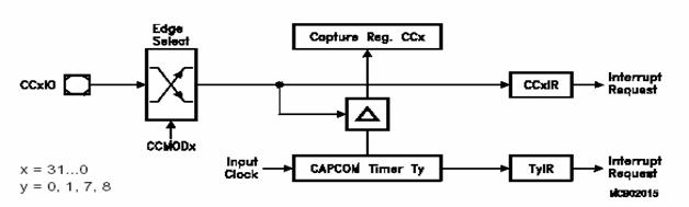
Capture Mode Block Diagram

In response to an external event the content of the associated timer (T0/T1 or T7/T8, depending on the used CAPCOM unit and the state of the allocation control bit ACCx) is latched into the respective capture register CCx . The external event causing a capture can be programmed to be either a positive, a negative, or both a positive or a negative transition at the respective external input pin CCxIO.
The triggering transition is selected by the mode bits CCMODx in the respective CAPCOM mode control register. In any case, the event causing a capture will also set the respective interrupt request flag CCxIR, which can cause an interrupt or a PEC service request, when enabled.
In order to use the respective port pin as external capture input pin CCxIO for capture register CCx, this port pin must be configured as input, ie. the corresponding direction control bit must be set to '0'. To ensure that a signal transition is properly recognized, an external capture input signal should be held for at least 8 CPU clock cycles before it changes its level. During these 8 CPU clock cycles the capture input signals are scanned sequentially. When a timer is modified or incremented during this process, the new timer contents will already be captured for the remaining capture registers within the current scanning sequence.If pin CCxIO is configured as output, the capture function may be triggered by modifying the corresponding port output latch via software, eg. for testing purposes.
Compare Mode 0 and 1 Block Diagram
Compare Mode 0
This is an interrupt-only mode which can be used for software timing purposes. Compare mode 0 is selected for a given compare register CCx by setting bit field CCMODx of the corresponding mode control register to '100B'.
In this mode, the interrupt request flag CCxIR is set each time a match is detected between the content of compare register CCx and the allocated timer. Several of these compare events are possible within a single timer period, when the compare value in register CCx is updated during the timer period. The corresponding port pin CCxIO is not affected by compare events in this mode and can be used as general purpose IO pin.
If compare mode 0 is programmed for one of the registers CC8...CC15 or CC24...CC31, the doubleregister compare mode becomes enabled for this register if the corresponding bank 1 register is programmed to compare mode 1 (see section "Double- Register Compare Mode").
Compare Mode 1
Compare mode 1 is selected for register CCx by setting bit field CCMODx of the corresponding mode control register to '101B'.
When a match between the content of the allocated timer and the compare value in register CCx is detected in this mode, interrupt request flag CCxIR is set to '1', and in addition the corresponding output pin CCxIO (alternate port output function) is toggled. For this purpose, the state of the respective port output latch (not the pin) is read, inverted, and then written back to the output latch. Compare mode 1 allows several compare events within a single timer period. An overflow of the allocated timer has no effect on the output pin, nor does it disable or enable further compare events.In order to use the respective port pin as compare signal output pin CCxIO for compare register CCx in compare mode 1, this port pin must be configured as output, ie. the corresponding direction control bit must be set to '1'. With this configuration, the initial state of the output signal can be programmed or its state can be modified at any time by writing to the port output latch.In compare mode 1 the port latch is toggled upon each compare event (see Timing Example above).
Note: If the port output latch is written to by software at the same time it would be altered by a compare event, the software write will have priority. In this case the hardware-triggered change will not become effective. If compare mode 1 is programmed for one of the registers CC0...CC7 or CC16...CC23 the doubleregister compare mode becomes enabled for this register if the corresponding bank 1 register is programmed to compare mode 0 (see section "Double-Register Compare Mode").
Note: If the port output latch is written to by software at the same time it would be altered by a compare event, the software write will have priority. In this case the hardware-triggered change will not become effective.On channels 24...27 compare mode 1 will generate interrupt requests but no output function is provided
Compare Mode 2 and 3 Block Diagram
Compare Mode 2
Compare mode 2 is an interrupt-only mode similar to compare mode 0, but only one interrupt request per timer period will be generated. Compare mode 2 is selected for register CCx by setting bit field CCMODx of the corresponding mode control register to '110B'.
When a match is detected in compare mode 2 for the first time within a timer period, the interrupt request flag CCxIR is set to '1'. The corresponding port 2 pin is not affected and can be used for general purpose IO. However, after the first match has been detected in this mode, all further compare events within the same timer period are disabled for compare register CCx until the allocated timer overflows. This means, that after the first match, even when the compare register is reloaded with a value higher than the current timer value, no compare event will occur until the next timer period.
In the example below, the compare value in register CCx is modified from cv1 to cv2 after compare event #1. Compare event #2, however, will not occur until the next period of timer Ty.
Compare Mode 3
Compare mode 3 is selected for register CCx by setting bit field CCMODx of the corresponding mode control register to '111B'. In compare mode 3 only one compare event will be generated per timer period.
When the first match within the timer period is detected the interrupt request flag CCxIR is set to '1' and also the output pin CCxIO (alternate port function) will be set to '1'. The pin will be reset to '0', when the allocated timer overflows. If a match was found for register CCx in this mode, all further compare events during the currenttimer period are disabled for CCx until the corresponding timer overflows. If, after a match was detected, the compare register is reloaded with a new value, this value will not become effective until the next timer period.In order to use the respective port pin as compare signal output pin CCxIO for compare register CCx in compare mode 3 this port pin must be configured as output, ie. the corresponding direction control bit must be set to '1'. With this configuration, the initial state of the output signal can be programmed or its state can be modified at any time by writing to the port output latch. In compare mode 3 the port latch is set upon a compare event and and cleared upon a timer overflow (see Timing Example above).However, when compare value and reload value for a channel are equal the respective interrupt requests will be generated, only the output signal is not changed (set and clear would coincide in this case).
Note: If the port output latch is written to by software at the same time it would be altered by a compare event, the software write will have priority. In this case the hardware-triggered change will not become effective. On channels 24...27 compare mode 1 will generate interrupt requests but no output function is provided.
CAPCOM Unit Block Diagram

A CAPCOM unit is typically used to handle high speed IO tasks such as pulse and waveform generation, pulse width modulation, or recording of the time at which specific events occur. It also allows the implementation of up to 16 software timers. The maximum resolution of the CAPCOM units is 400 ns (@ 20 MHz CPU clock).Each CAPCOM unit consists of two 16-bit timers (T0 / T1 in CAPCOM1, T7 / T8 in CAPCOM2),each with its own reload register (TxREL), and a bank of sixteen dual purpose 16-bit capture/
compare registers (CC0 through CC15 in CAPCOM1, CC16 through CC31 in CAPCOM2).The input clock for the CAPCOM timers is programmable to several prescaled values of the CPU clock, or it can be derived from an overflow/underflow of timer T6 in block GPT2. T0 and T7 may also operate in counter mode (from an external input) where they can be clocked by external events.
Each capture/compare register may be programmed individually for capture or compare function, and each register may be allocated to either timer of the associated unit. Each capture/compare register has one port pin associated with it which serves as an input pin for the capture function or
as an output pin for the compare function (except for CC27...CC24 on P1H.7...P1H.4, which only provide the capture function). The capture function causes the current timer contents to be latched into the respective capture/compare register triggered by an event (transition) on its associated port pin. The compare function may cause an output signal transition on that port pin whose associated capture/compare register matches the current timer contents. Specific interrupt requests are generated upon each capture/compare event or upon timer overflow. The figure below shows the basic structure of the two CAPCOM units.
Note: The CAPCOM2 unit provides 16 capture inputs, but only 12 compare outputs.
The CAPCOM Timers
The primary use of the timers T0 / T1 and T7 / T8 is to provide two independent time bases (400 ns maximum resolution @ 20 MHz CPU clock) for the capture/compare registers of each unit, but theymay also be used independent of the capture/compare registers.The basic structure of the four timers is identical, while the selection of input signals is different for timers T0/T7 and timers T1/T8 (see figures below).
Capture Mode Block Diagram
In response to an external event the content of the associated timer (T0/T1 or T7/T8, depending on the used CAPCOM unit and the state of the allocation control bit ACCx) is latched into the respective capture register CCx . The external event causing a capture can be programmed to be either a positive, a negative, or both a positive or a negative transition at the respective external input pin CCxIO.
The triggering transition is selected by the mode bits CCMODx in the respective CAPCOM mode control register. In any case, the event causing a capture will also set the respective interrupt request flag CCxIR, which can cause an interrupt or a PEC service request, when enabled.In order to use the respective port pin as external capture input pin CCxIO for capture register CCx, this port pin must be configured as input, ie. the corresponding direction control bit must be set to '0'. To ensure that a signal transition is properly recognized, an external capture input signal should be held for at least 8 CPU clock cycles before it changes its level.During these 8 CPU clock cycles the capture input signals are scanned sequentially. When a timer is modified or incremented during this process, the new timer contents will already be captured for the remaining capture registers within the current scanning sequence. If pin CCxIO is configured as output, the capture function may be triggered by modifying the corresponding port output latch via software, eg. for testing purposes.
Compare Mode 0 and 1 Block Diagram

Compare Mode 0
This is an interrupt-only mode which can be used for software timing purposes. Compare mode 0 is selected for a given compare register CCx by setting bit field CCMODx of the corresponding mode control register to '100B'.
In this mode, the interrupt request flag CCxIR is set each time a match is detected between the content of compare register CCx and the allocated timer. Several of these compare events are possible within a single timer period, when the compare value in register CCx is updated during the timer period. The corresponding port pin CCxIO is not affected by compare events in this mode and can be used as general purpose IO pin. If compare mode 0 is programmed for one of the registers CC8...CC15 or CC24...CC31, the doubleregister compare mode becomes enabled for this register if the corresponding bank 1 register is programmed to compare mode 1 (see section "Double- Register Compare Mode").
Compare Mode 1
Compare mode 1 is selected for register CCx by setting bit field CCMODx of the corresponding mode control register to '101B'.
When a match between the content of the allocated timer and the compare value in register CCx is detected in this mode, interrupt request flag CCxIR is set to '1', and in addition the corresponding output pin CCxIO (alternate port output function) is toggled. For this purpose, the state of the respective port output latch (not the pin) is read, inverted, and then written back to the output latch. Compare mode 1 allows several compare events within a single timer period. An overflow of the allocated timer has no effect on the output pin, nor does it disable or enable further compare events.In order to use the respective port pin as compare signal output pin CCxIO for compare register CCx in compare mode 1, this port pin must be configured as output, ie. the corresponding direction control bit must be set to '1'. With this configuration, the initial state of the output signal can be programmed or its state can be modified at any time by writing to the port output latch. In compare mode 1 the port latch is toggled upon each compare event (see Timing Example above).
Note: If the port output latch is written to by software at the same time it would be altered by a compare event, the software write will have priority. In this case the hardware-triggered change will not become effective. If compare mode 1 is programmed for one of the registers CC0...CC7 or CC16...CC23 the doubleregister compare mode becomes enabled for this register if the corresponding bank 1 register is programmed to compare mode 0 (see section "Double-Register Compare Mode"). Note: If the port output latch is written to by software at the same time it would be altered by a compare event, the software write will have priority. In this case the hardware-triggered change will not become effective. On channels 24...27 compare mode 1 will generate interrupt requests but no output function is provided.
Compare Mode 2 and 3 Block Diagram

Compare Mode 2
Compare mode 2 is an interrupt-only mode similar to compare mode 0, but only one interrupt request per timer period will be generated. Compare mode 2 is selected for register CCx by setting bit field CCMODx of the corresponding mode control register to '110B'.When a match is detected in compare mode 2 for the first time within a timer period, the interrupt request flag CCxIR is set to '1'. The corresponding port 2 pin is not affected and can be used for general purpose IO. However, after the first match has been detected in this mode, all further compare events within the same timer period are disabled for compare register CCx until the allocated timer overflows. This means, that after the first match, even when the compare register is reloaded with a value higher than the current timer value, no compare event will occur until the next timer period.
In the example below, the compare value in register CCx is modified from cv1 to cv2 after compare event #1. Compare event #2, however, will not occur until the next period of timer Ty.
Compare Mode 3
Compare mode 3 is selected for register CCx by setting bit field CCMODx of the corresponding mode control register to '111B'. In compare mode 3 only one compare event will be generated per timer period.When the first match within the timer period is detected the interrupt request flag CCxIR is set to '1' and also the output pin CCxIO (alternate port function) will be set to '1'. The pin will be reset to '0', when the allocated timer overflows.If a match was found for register CCx in this mode, all further compare events during the current timer period are disabled for CCx until the corresponding timer overflows. If, after a match was detected, the compare register is reloaded with a new value, this value will not become effective until the next timer period.In order to use the respective port pin as compare signal output pin CCxIO for compare register CCx in compare mode 3 this port pin must be configured as output, ie. the corresponding direction control bit must be set to '1'. With this configuration, the initial state of the output signal can be programmed or its state can be modified at any time by writing to the port output latch.In compare mode 3 the port latch is set upon a compare event and and cleared upon a timer overflow (see Timing Example above).
However, when compare value and reload value for a channel are equal the respective interrupt requests will be generated, only the output signal is not changed (set and clear would coincide in this case).
Note: If the port output latch is written to by software at the same time it would be altered by a compare event, the software write will have priority. In this case the hardware-triggered change will not become effective. On channels 24...27 compare mode 1 will generate interrupt requests but no output function is provided.
|
