Read me first 1. The "LOAD SETUPD EFAULTS" function loads the system default data directly from ROM and initializes the associated hardware properly . This function is Necessary When you accept this mainboard ,
LOAD SETUP DEFAULT 2. KBPO(Key Board Power On) Function : There is a basic requirement that the "+5V SB"power of the ATX power supply must be>=0.1A(100Ma). Package Checklist Please check your package which should include all items listed below. If you find any item damaged or missed , please contact your supplier. l One floppy ribbon cable l One Parallel port ribbon cable l One Serial port ribbon cable(COM1,COM2)
Contents page Chapter 1-Introduction.....................31-1 Notice........................4 Chapter 2-Hardware Design...................52-1 Mainboard Layout...................7 2-2 Jumpers/connectors settings................8 2-3 System Memory Configuration............. ..18 2-4 ATX Power ON/OFF Control................19 2-5 Extemal Modem Ring-in ON Functions................... ...20Chapter 3-Award BIOS Setup..................20 3-1 Standard CMOS Setup..................21 3-2 BIOS Features Setup..................22 3-3 Chipset Features Setup..................27 3-4 Power Management Setup................30 3-5 PNP/PCI Configuration.................34 3-6 Load Setup Detectios..................36 3-7 Integrated Periphera....................36 3-8 Change Supervisor or User Password..............40 3-9 IDE HDD Auto Detection.................41 3-10 HDD LOWLEVEL FOR 121v2112b MAT.................44 3-11 Save & Exit Setup.....................44
Chaper 1 IntroductionThis mainboard is a high performance system hardware based on Intel Pentium processor and is equipped with an AGP slot , three PCI slots, Three standard ISA slots , Super Multi-I/O controller and dual port PCI -IDE connectors for the future expansion .The hardware dimension is 220mm x 230mm with MVP3 dual Design and a four-layer-design technology . Specification technology , AMD K5/K6/K6-2/K6-3 , Cyrix 6x86L/6x86MX & idt C6 operating at 120~500MHZ with 321 ZIF socket 7 provides scalability to accept faster Processors in the future . SOCKET x2 & 72 -Pin SIMM SOCKET x2) . lot and Provides two independent high performance PCI IDE interfaces capable of supporting PIO Mode 3/4 and Ultra-DMA33 devices . ports(16550 Fast UART compatible) , 1USB Connector , a PS/2 style mouse connector and an AT style keyboard connector .
l Supports CPU Hardware sleep , APM (Advanced Power Management) and ACPI (Advanced Configuration Power Interface) . l Supports an ATX power supply connector for a Remote On/Off , a phone- Ring power On and a Keyboard power On Function . l Supports Switching Regulator for CPU power supply . l Support hardware monitor function .
1-1 Notice : 一. This mother board adept Chips Design MVP3(VT82C598MVP) . P5MVP3 difference : 1.
P5MVP3 (VT82C598MVP) 60MHZ~100MHZ : Bus clock (Support 100MHZ) 二. When you adjust 100MHZ on P5MVP3 Suggest you use DIMM module . Because The DIMM and SIMM is mixed. If The SIMM timing Is not the same with DIMM, maybe Can,t match with DIMM.
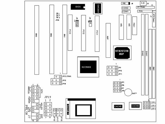
Chapter 2 Hardware design2-1 Mainboard LayoutThis mainboard is designed with VIA ApolloMVP3 AGP/PCIset chipset which is developed by VIA Corporation to fully support Pentium Processor PCI/ISA system . By providing a massive increase in the bandwidth available between the video card and the processor (66MHZ) , the unique feature of AGP supported by VIA Apollo MVP3 chipset improves the speed of rendering and texturing for 3D graphics. The chipset also provides an integrated IDE controller with two high Performance IDE interfaces for up to four IDE devices (hard devices , CD-ROM device , etc) .The SMSC37C669 Super I/O controller provides the standard PC I/O function: one floppy interfacd , two 16 Byte FIFO serial ports and one EPP/ECP capable parallel port . This mainboard layout is shown in the next page for user,s reference . care must be taken when inserting memory modules, CPUs or even plugging PCI card into associated slots to avoid damaging any circuits or sockets on board. A cooling fan is strongly recommended when installing Pentium/Pentium MMX/K5/K6/K6-2/K6-3/6x86/ 6x86L/ 6x86MX/C6 processor due to possible overheat .This mainboard supports a minimum of 8MB and a maximum of 512MBof system Memory while Onboard 512KB cache to increase system performance .
This mainboard supports standard Fast Psge, or 60ns This mainboard supports two Onboard PCI IDE connectors , and automatically detects IDE harddisk type by BIOS utility automatic .This mainboard supports A ward Plug & Play BIOS for the ISA and PCI cards . The BIOS can be located in Flash EPROM which can replace BIOS code easily if neces-sary
P5MVP3 Layout
Figure 2-1
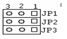
2-2 Jumpers/Connectors SettingsThis section describes some of the connectors on the mainboard . 一. PRN1-Parallel PortThis mainboard provides a 2 x 13-pin parallel port connector . 二. COM1/COM2-Serial Port ConnectorsThis mainboard provides two 2 x 5-pin serial port connectors . COM1 and COM2 . 三. This mainboard has a 2 x 17-pin floppy drive connector . 四. IDE1/IDE2-Primary/Secondary IDE Connectors This mainboard has a 32-bit Enhanced PCI IDE Controller that Provides two connectors, IDE0 (primary) and IDE1 (secondary) . 五. Jumper Setting : JP1: 1-2 (5V For ISSI TAG RAM) 2-3 (3.3V For UMC TAG RAM) JP2: 1-2 (Reserved) 2-3 For 512k cache JP3: 1-2 Interleave Burst 2-3 linear Burst
1.DRAM clock adjust
2. The system Bus clock Jumper setting
※ When you adjust CPU Bus clock to 100MHZ The SDRAM has to can support 100MHZ timming JP12:CPU Fan connector
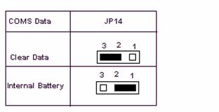
JP14:Clear CMOS DataClear the CMOS memory by shorting this jumper momentarily;
JP16~JP18:CPU Speed selectors
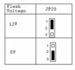
JP20:Flash ROM Voltage Select
JP19:CPU Vcore voltage selection : For Pentium Processor with MMX technology AMD K6 and cyrix 6x86L/6x86MX JP19(Vcore voltage setting)
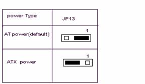
For the CPU everytime that you install a CPU , and , make sure that your JP19 is matched with the CPU voltage , otherwise will damage the CPU or make the system unstable . 2. When the new CPU is announced and is not listed on this manual , please refer to the above table , select the correct voltage setting for it . J1:ATX Style Power Connector The ATX power supply a single 20-pin connector .
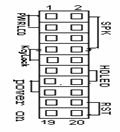
Software Power-Off Follow the steps below to use the "Software Power-Off Control" function in Windows 95 with ATX power supply . 1.Click the START button on the Windows 95 task bar . 2.Select Shut Down The Computer to turn off the computer . The message "It is now safe to turn off your computer ."will not be shown when using this function . J7(13,15)(PWR ON)-Power Button & Suspend Switch Connector When the system is turned off , push the power button to turn the system back on . When the system is on , push the power button rapidly to switch the system to the Suspend mode , and , by pushing and holding the button for more than 4 seconds to turn the system completely off . When the system is in the Suspend mode , push the power button rapidly to turn the system on . J2:AT Power - Power Supply Connector This power supply connector has two sets of six-wire connectors . Plug the dual connectors onto the board and make sure that the black leads are in the center .
Note: Before connecting the power supply , make sure it is not
14 J3:Keyboard Connector A 5-pin female DIN keyboard connector is located at the upper Right corner of the mainboard . Plug the keyboard jack directly into this connector .
Attach mouse cable to this 5-pin connector .
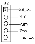
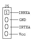
The system board provides a 4-pin infrared connector-J5 as an optional module for wireless transmitting and receiving .
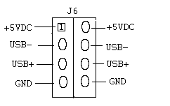
15 16 J6:USB Connector
J7-Pin Description
The speaker connector is a 4-pin connector for connecting the system and the speaker . J7(1,3,5,7,9) (Key-Lock)- Keylock & power LED Connector
J7(12,14) (HD-LED)-HDD LED Connector
Attach the cable of hard disk drive LED to this connector . The LED lights when an HDD is active . J7(18,20) (RST)-Reset Switch Connector Attach the reset push button cable to this connector
The system board has a 2-pin connector for rebooting your Computer without having to tun off your power switch . This Prolongs the life of the system,s power supply .
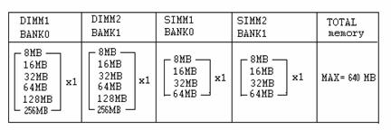
17 18 2-3 System Memory Configuration This mainboard supports different type of settings for the system memory .
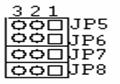
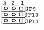
This mainboard supports 2 Kinds of powerful and flexible SDRAM frequency selections . These can be synchronous with CPU bus clock or fixed as 66MHZ. By implementing the VCS (Virtual Clock Synchronization)technology , this mainboard refers to the use of delay-lcok-loop(DLL) to enable synchronous and pseudo-synchronous operation of the processor and DRAM , AGP and PCI buses . The JP5,JP9 allows user to set the SDRAM Frequency between 66/100MHZ . SDRAM Clock select
Jumper,s position: Notice:When you adjust 100MHZ . Please only use DIMM module (Recommanded), Because the DIMM and SIMM both be installed The SIMM timing is not the same maybe can,t match with DIMM. JP5(2-3),JP9(1-2): Pseudo-synchronous Status(Fixed as 66MHZ) A more stable and compatible operation condition for non-100MHZ based SDRAM when you are using 100MHZ based CPU . This setting is suitable for those users who are like to remain the usage of current SDRAM module . JP5(1-2),JP9(2-3),JP10(1-2),JP11(2-3): Synchronous Status(SDRAM Clock = CPU Bus Clock Increasing the bus speeds from the traditional 66MHZ to 100MHZ greatly improves system performance because the speed at which data traveling between the CPU and memory is increased by 50% . However , there is one thing you should bear in mind . Please make sure you are using 125MHZ(-8) based or above SDRAM module. 2-4 ATX Power ON/OFF Control This mainboard equips an ATX power connector which is a single 20-PIN input device for an ATX power supply . An ATX power supply provides a build-in remote Power ON/OFF function . To implement the function , a momentary switch which is nomally open should be connected to the position J7 (PIN 13, 15) as the system ,s power ON/OFF button . Note that an AT power supply does not offer this function . Based on the ATX power connector , this mainboard has been designed to support both ACPI and Soft-OFF functions . According to the definition of ACPI , a Suspend mode will be enabled while you push the J7(system power ON/OFF) button less than 4 seconds . Nevertheless , the system will
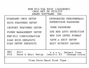
19 Soft-OFF(coming from this mainboard circuit controller) , it is another way to turn off your system . Your system can be shut down automatically by an operation system such as Windows 95 . 2-5 External Mode Ring-in Power ON Functions On The basts of bounded functions in I/O Chipset , the serial ports are able to Support the Extemal Modem Ring-in Power On function. Once user connect the Extemal modem to COM1 or COM2, this mainbard mainboard allows user to turn On their system through the remote and host,s dial-up control. Chapter 3 AWARD BIOS SETUP Award,s ROM BIOS provides a built-in setup program which allows user to modify the basic system configurations and hardware parameters . The modified data will be stored in a battery-backed CMOS RAM so that data will be retained even when the power is turned off .In general , the information saved in the CMOS RAM stays unchanged unless there is a configuration change in the system , such as a hard drive replacement or a new device installation . If this does happen , you will need to reconfigure your configuration parameter . To Enter Setup Program Power
on the computer and press <
20
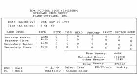
Figure3-1 CMOS SETUP UTILITY The menu displays all major selection items . Select the item you need to reconfigure .The selection is made by moving cursor (press any direction key ) to the item and press the 'Enter' key . An on-line help message is displayed at the bottom of the screen as the cursor is moving to various items which provides a better understand-ing of each function . When a selection is made , the menu of selected item will appear so the user can modify the associated configuration parameters . 3-1 STANARD COMS SETUP Choose "STANDARD COMS SETUP" in the CMOS SETUP UTILITY Menu(Fig3-1) The STANDARD CMOS SETUP Allows user to configure system setting such as the Current date and time , type of hard disk installed , floppy type , and display type . Memory
21 a field is Highlighted(use direction keys to move cursor and <Enter> key to select),the entries in theField will be changed by pressing <pgDn> or<PgUp>keys
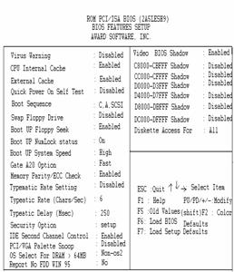
or user can enter new data directly From the keyboard . Figure3-2 STANDARD CMOS SETUP NOTE:If the Primary Master/Slave and the Secondary Master/Slave are set as "Auto", the hard disk size and model will be auto-detected . NOTE:The "Halt On:"field is to determine when to halt the system by the BIOS if an error occurrs. 3-2 BIOS FESTURES SETUP By selecting the "BIOS FEATURES SETUP" option in the CMOS SETUP UTILITY Menu , user can change system related parameters in the displayed in the displayed menu .This menu shows all of the manufacturer,s default values of this mainboard . Again , user Can move the cursor by pressing direction keys and <PgDn>or<PgUp>keys to modify
22 Figure3-3 BIOS FEATURES SETUP Note: The Security Option contians "setup" and "system" .The "setup" indicates that the password setting is for CMOS only while the "system " indicates the pass- word setting is for both CMOS and system boot up . l Virus Warning :This category flashes on the screen . During and after the system boots up. Any attempt to write to the boot sector or partition table of the hard disk drive will halt the system and an error message will appear . You should then run an anti-virus program to locate the virus program to locate the virus . Keep in mind that this feature protects only the boot sector , not the entire hard drive . Default value is Disabled .
23 Message to appear when any attempt to access the boot sector or hard disk partition table . Disabled : No warning message to appear when any attempt to access the boot sector or Hard disk partition table . l CPU Internal Cache/External Cache : These two categories speed up Memory access . However , it depends on CPU/chipset design .The default value is Enabled . If your CPU is without Internal Cache then this item "CPU Internal Cache" will not be shown . Enabled : Enable cache . Disabled : Disable cache . l Quick Power On Self Test : This category speeds up Power On Self Test(POST) after you power on the computer . If it is set to Enable , BIOS will shorten or skip some checking items during POST. Enabled : Enable quick POST. Disabled: l Boot Sequenec : This category determines which drive is searched first for the O/S(Operating System) . The default value is A,C . A,C : The system will search for floppy disk drive first then hard disk drive . C,A : The system will search for hard disk drive first then floppy disk drive . Swap Floppy Drive : This will swap your physical drive letters A & B if you are using two floppy disks . The default value is Disabled . Enabled : Floppy A & B will be swapped under the O/S . Disabled : Floppy A & B will be not swapped . l Boot Up Floppy Seek : During Power-On-Self-Test(POST),BIOS
24 Installed floppy drive is 40 or 80 tracks . Only 360K type is 40 tracks while 760K , 1.2M and 1.44M are all 80 tracks . The default value is Enabled . Enabled : BIOS searches for floppy disk drive to determine if it is 40 or 80 tracks . Note that BIOS can not tell from 720K , 1.2M or 1.44M drive type As they are all 80 tracks. Disabled :BIOS will not search for the type of floppy disk drive by track number .Note that there will not be any warning message if the drive installed is 360K . l Boot Up NumLock Status : The default value is On . On :Keypad is number keys . Off : Keypad is arrow keys . l Boot UP System Speed : Select default system speed . The system will run at the Selected speed after the system boots . High : Set the speed to high . Low :Set the speed to low . l Gate A20 Option : This refers to the way the system addresses memory above 1MB (extended memory). The default value is Fast . hardware. Fast : The a20 signal is controlled by Port 92 or chipset specific method . l Typematic Rate Setting :This determines the typematicr rate . Enabled :Enable typematic rate and typematic delay programming . Disabled : Disable typematic rate and typematic delay programming . The system BIOS will use defualt value of 2 items and the default is controlled by the Keyboard .
25 l Typematec Rate(Chars/Sec): 6 : 6 characters per second . 8: 8 characters per second. 10:10 characters per second . 12:12 characters per second. 15:15 characters per second . 20:20 characters per second. 24:24 characters per second. 30:30 characters per second. l Typematic Delay(Msec) : This determines the time between the first and second Character displayed , when holding a key . 250 :250msec. 500:500 msec. 750:750 msec. 1000:1000 msec. l Security Option :This category allows you to limit access to the system and Setup, or just or Setup. The default value is Setup . System : The system will not boot and the access to Setup will be denied if the correct password is not entered at the prompt . Setup : The system will boot , but the access to Setup will be denide if the correct password is not entered at the prompt . l PCI/BGA Palette Snoop :This filed controls the ability of a primary PCI VGA Conntroller to share a common palette (when a snoop write cycles) with an ISA Video card . The default value is Disabled . Enabled : If an ISA card connects to a PCI VGA card via the VESA connector and the ISA card connects to VGA monitor and uses the RAMDAC of PCI card , the PCI/VGA Palette Snoop is
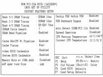
26 Disabled : Disable the VGA card Palette snoop function . l Video BIOS Shadow :It determines whether video BIOS will be copied to RAM . However , it is optional from chipset design . Video Shadow will increase the video Speed. Enabled : Video shadow is enabled . Disabled: Video shadow is disabled . l C8000 - CBFFF Shadow : CC000 - CFFFF Shadow : D0000 - D3FFF Shadow : D4000 - D7FFF Shadow : D8000 - DBFFF Shadow : DC000 - DFFFF Shadow : These categories determine whether optional ROM will be copied to RAM by 16K byte or 32Kbyte per unit and the size depends on the chipset . Enabled : Optional shadow is enabled. Disabled : Optional shadow is disabled . 3-3 CHIPSET FEATURES SETUP Choose the "CHIPSET FEATURES SETUP" in the CMOS SETUP UTILITY Menu to display the following menu .
27 Note : When you insert slower memery modules in the system and set a faster timing , maybe the system will hang up. l DRAM Timing :The default value is 60ns. 60ns :
2 (faster) Mode/EDO DRAM. 70ns: 3 (slower) Burst Wait Slate , for 70ns page Mode/EDO DRAM. l SDRAM Cycle length: The default value is 2. 2:2 HCLKS. 3:3 HCLKS. l DRAM Read Pipeline :The default value is Enabled. Disabled : Enabled :This field enableds the pipelining of DRAM read cycle. l Cache RD+CPU Wt Pipeline: The default value is Enabled. Disabled : Enabled :This field enableds the pipelining of Cache reads and CPU writes cycle. l Cache Timing :The default value is fastest. Fast :Cache burst mode timing =3 1 1 1 2 1 1 1. Fastest : Cache burst mode timing=3 1 1 1 1 1 1 1. l Video BIOS Cacheable :The default value is Enabled. Enabled :Enabled the Video BIOS Cacheable to speed up the VGA Performance. Disabled :
28 l System BIOS Cacheable : The default value is Eisabled . Enabled :Allow caching of the system BIOS ROM at F0000h-FFFFFh. Disabled : l Memory Hole at 15M-16M :The default value is Disabled. Disabled : Enabled :This field enableds the main memory(15~16MB) remap to ISA BUS. l AGP Aperture Size :The amount of the system memory that the AGP card Is allowed to share .The options available are4M,8M,16M, 32M, 64M, 128M,256M.The default value is 64M. l Onchip USB:Enabled USB Keyboard Support : Enabled Enabled :Enabled USB Keyboard. l System/CPU Warning Temp : The default value 60℃/140℉. Disabled : Enabled : The options available is 50℃/122℉~70℃/158℉. l Current CPU Temp : This is the current temperature of the CPU.
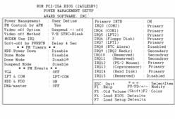
3-4 POWER MANAGEMENT SETUP Choose the "POWER MANAGEMENT SETUP" in the CMOS SETUP UTILITY to display the following screen . This menu allows the user to modify the power management parameters and IRQ signals . In general , these parameters should not be changed unless it is
Figure3-5 POWER MANAGEMENT SETUP Again , users can move the cursor by pressing direction keys to the field needed to be Modified and press <PgDn>or<PgUp>to alter item selection. You can only changeThe content of Doze Mode, Standby Mode, and Suspend Mode when the PowerManagement is set to 'User Define'. 3-4-1 The Description of the Power Management A. Power Management mode selection: Disabled :The
system operates in (Non-GREEN) And the Power Management function is disabled.
29 30 Min.saving :This mode will minimize the power saving capability. User define :Allow user to define time-out parameters to control power saving mode .Refer to item B shown below. HDD Standby HDD Standby timer can be set from 1 to 15 mimute(s). System Doze The "System Doze" mode timer starts to count when there is no "PM events" occurred. The valid time-out setting is from 1 mimute up to 1hour. System Suspend This function works only when the Pentium Procssor is installed . The timer starts to count when "System Standby" mode timer is timed out and no "PM Events" occurred. Valid range is from 1 minute up to 1hour. 3-4-2 Description of the Green Functions This mainboard supports HDD power Down, Doze and Suspend power saving Functions . The detailed description of these functions is provided in the next page. l PM Controlby APM If Advanced Power Management(APM) is installed on your system , selecting Yes gives better power savings. l Video Off Method Determines the manner in which the monitor is blanked.
31 synchronization ports and writes blanks to the video buffer. DPMS Support:Select this option if your monitor supports the Display Power Management Signaling (DPMS) standard of the Video Electronics Standards Association(VESA).Use the softw are supplied for your video subsystem to select video power Management values. Blank Screen:System only writes blanks to the video buffer. l Video off Option Determines whin to activate the video off feature for monitor power management. The settings are Video off after Suspend/standby/Doze/(N/A). l Soft-off by PWRBTN This field is for the soft-off function setting. When the board utilizes an ATX Power supply , two types of settings are offered: Delay 4 Sec. And instant-off. When the setting is Delay 4 Sec, users can power off the system by pressing POWER-ON button(J7) for 4 seconds. However, if users press POWER-ON Button for less than 4 seconds, the system will enter the Suspend Mode. When Tee setting is instant-Off, users first press on POWER-ON button will power off the system, but the second press will power on the system. HDD Standby Mode When system stops reading or wiriting HDD, the timer starts to count . The system Will cut off the HDD power when timer runs out of time .
32 write to HDD command is executed again. Doze Mode The system hardware will drop down CPU clock from nomal working speed When Doze mode time-out occurs. Suspend Mode When the system suspend timer times out , the system will enter the suspend mode And the chipset will stop CPU clock immediately .The power consumption in Suspend Mode is lower than in standby mode. The screen is also blanked out. PMEvents: AWARD BIOS defines 7 PM Events in the power management mode (Doze & Suspend). The user can initialize any PM Events to be "Enable" or "Disable". When the system detects all of the enabled ebents do not habe any activity, It will start the system Doze timer first if the "Power Management" is not "Disabled". Once the system Doze timer is timed out , it will process doze power saving procedure by starting the system suspend timer. When the suspend timer times out , all of the CPU clock will stop by dropping system clock down tozero and remains this way until any one of the "Enabled "event occrrs.
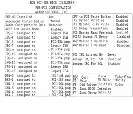
33 34 3-5 PNP / PCI CONFIGURATION The PNP /PCI configuration program is for the user to modify the PCI/ISA IRQ signals When various PCI/ISA cards are inserted in the PCI or ISA slots. WARNING :Any misplacing IRQ could cause system cant,t pick
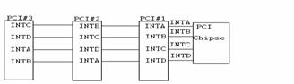
Figure3-6PCICONFIGURATIONSETUP Resource Controlled By:The default value is Manual. Manual: The field defines that the PNP Card,s resource is controlled by manual. You can setup whether IRQ-X or DMA-X is assigned to PCI/ISA PNP Or legacy ISA Cards. Auto: If your ISA card and PCI card are all PNP card. Set this field to "Auto" The BIOS will assign the interrupt resource automatically. l Reset Configuration Data:The default value is Disabled. Disabled: Enabled:If you plug some Legacuy cards in the system and record into ESCD (Extended System Configuration Data). You can set this field to be Enabled and to clear ESCD at one time, when some Legacy cards are Removed. l PCI IDE IRQ Map To:The default value is PCI/AUTO. When you have true PCI card(s) plugged into the system , you will not need to change any thing here in the SETUP program. However, if you do not Know whether you are using a true PCI card, please refer to your PCI Card user,s manual for the details. When you have a Legacy card (described in section 2-5) to plug Into the system ,a proper setting is extremely important or it may cause The system hung up. The diagram shown below tells you how the Rotating Priority Mechanism is designed.
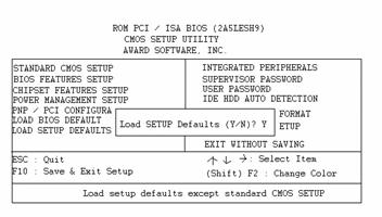
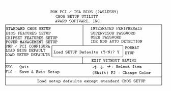
35 36 3-6 LOAD SETUP DEFAULTS The "LOAD SETUP DEFAULTS" function loads the system default data directly from ROM and initializes the associated hardware properly.
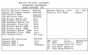
Figure 3-8 LOAD SETUP DEFAULT 3-7 INTEGRATED PERIPHIERALS
(PCI or ISA card)IDE connector. You have to set Onboard Primary PCI IDE, Disabled and Onboard Secondary PCI IDE: Disabled From CHIPSETF EATURESS ETUP UTILIIY. The Onboard PCI IDE cable should be equal to or less than 18 inches(45cm).IDE HDD Block Mode: The default value is Enabled. Enabled: Enabled IDE HDD Block Mode. The HDD transfer rate is better than Disable. Disabled: Disable IDE HDD Block Mode. l PCI Slot IDE 2nd Channel: The default value is Enabled. Enabled :Enable secondary IDE port and BIOS will assign IRQ15 for this port. Disabled :Disable secondary IDE port and IRQ15 is available for other device. l Onboard Primary PCI IDE: The default value is Enabled. Enabled :Enable Onboard 1 st channel IDE port. Disabled: Disable Onboard 1 st channel IDE port .When use On-card (PCI or ISA Card) IDE connector. l Onboard Secondary PCI IDE: The default value is Enabled. Enabled:Enable Onboard 2nd channel IDE port. Disabled :Disable Onboard 2nd channel IDE port When use On-card (PCI or ISA Card) IDE connector. l IDE Primary Master PIO:The default value is Auto. Auto :BIOS will automatically detect the Onboard Primary Master PCI IDE HDD Accessing mode. Mode0~4:Manually set the IDE Accessing mode. l IDE Primary Slave PIO:The default value is Auto.
37 IDE HDD Accessing mode. Mode0~4 : Manually set the IDE Accessing mode. l IDE Secondary Master PIO :The default value is Auto. Auto : BIOS will automatically detect the Onboard Secondary Master PCI IDE HDD Accessing mode. Mode0~4:Manually set the IDE Accessing mode. l IDE Secondary Slave PIO :The default value is Auto. Auto : BIOS will automatically detect the Onboard Secondary Slave PCI IDE HDD Accessing mode. Mode0~4:Manually set the IDE Accessing mode. l Onboard FDCController :The default value is Enabled. Enabled : Enable the Onboard floppy drive interface controller. Disabled :Disable the Onboard floppy drive interface controller, When using On-card ISA FDC,s controller. l Onboard UART1:This field allows the user to sellect the serial port. The default Value is 3F8H/IRQ4. COM1:Enable Onboard Serial port1 and address is 3F8H/IRQ4 COM2:Enable Onboard Serial port1 and address is 2F8H/IRQ3 COM3: Enable Onboard Serial port1 and address is 3F8H/IRQ4 COM4: Enable Onboard Serial port1 and address is 2F8H/IRQ3 Disabled:Disable Onboard Serial port 1. l Onboard UART2:This field allows the user to sellect the serial port. The default Value is 2F8H/IRQ3. COM1:Enable Onboard Serial port2 and address is 3F8H/IRQ4
38 COM3: Enable Onboard Serial port2 and address is 3F8H/IRQ4 COM4: Enable Onboard Serial port2 and address is 2F8H/IRQ3 Disabled:Disable Onboard Serial port 2 l Onboard UART 2 Mode: The default value is standard .This field allows the User toSelect the COM2 port that can support a serial Infrared Interface. Standard:Support a Support a Serial Infrared Interface IrDA. HPSIR:Support a HP Serial Infrared Interface format. ASKIR:Support a Sharp Serial Infrared Interface format. l Onboard Parallel port:This field allows the user to sellect the LP port. The default Value is 378H/IRQ7. 378H :Enable Onboard LPT port and address is 378H and IRQ7 278H : Enable Onboard LPT port and address is 278H and IRQ5 3BCH : Enable Onboard LPT port and address is 3BCH and IRQ7 Disabled :Disable Onboard LPT port. NOTE:Parallel Port address is 378H/3BCH that selects the rounting of IRQ7 for LPT1. Parallel Port address is 278H that selects the rounting of IRQ5 for LPT1. l Parallel port Mode :This field allows the user to sellect the parallel port mode. The default value is ECP+EPP. Normal :Standard mode, IBM PC/AT Compatible bidirectional parallel port. EPP :Enhanced Parallel Port mode. ECP :Extended Capability Port mode. EPP+ECP :ECP Mode&EPP Mode.
39 The ECP mode .The default value is DMA3. DMA1 :The filed selects the rounting of DMA1 for the ECP mode. DMA3 :The filed selects the rounting or DMA3 for the ECP mode. 3-8 CHANGE SUPERVISOR or USERPASSWORD To change the password, choose the "SUPERVISOR PASSWORD or USER PASS- WORD" option from the CMOS SETUP UTILITY menu and press[Enter]. NOTE:Either "Setup"or "System" must be selected in the "Security Option" of the BIOS FEATURES SETUP menu(Refer to Figure3-3 for the details). he ROM Will be used. The screen will display the following message. Enter Password: Press the [Enter]key to continue after proper password is given. change Default password, the SETUP UTILITY will display message and ask for a Confirmation. Confirm Password: or current Password (user-defined password), the user can change the password and store new One in CMOS RAM. A maximum of 8characters can be entered.
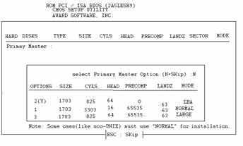
40 3-9 IDE HDD AUTO DETECTION The "IDE HDD AUTO DETECTION" utility is a very useful tool especially when you Do not know which kind of hard disk type you are using . You can use this utility to detect the correct disk type installed in the system automatically . But now you can set HARD DISK TYPE to Auto in the STANDARD CMOS SETUP. You do not need the"IDE HDD AUTO DETECTION"utility.The BIOS will Auto-detect the hard disk size and model on Display during POST.
NOTE:HDD Modes The Award BIOS supports 3 HDD modes:NORMAL,LBA and LARGE NORMAL mode. Generic access mode that is neither the BIOS nor the IDE controller will make transformations during accessing. The maximum nunbers of cylinders,head§ors for NORMAL mode are 1024,16 and 63. no Cyclinder (1024) x no.Head ( 16 ) x no.Sector ( 63 ) x no.per sector (512 )
528 Megabytes If an user sets the HDD to NORMAL mode. The maximum accessible HDD Size Will be 528 Megabytes even though its physical size may be greater than that! LBA(Logical Block Addressing) mode:This is a new HDD accessing method to Overcome the 528 Megabyte bottleneck. The number of cylinders,heads and sectors shown in the setup may not be the nunber Physically contained in the HDD. During the HDD accessing ,the IDE controller will transform the logical address Described by sector, head and cylinder into its own physical address inside the HDD. The maximun HDD size supported by LBA mode is 8.4 Gigabytes which is Obtained by the following formula: no Cyclinder (1024) x no.Head ( 255 ) x no.Sector ( 63 ) x bytes per secttor (512 )
41 42 LARGE mode:This is an extended HDD access mode supported by Award Software. Some IDE HDDs contain more than 1024 cylinders without LBA support( in some Cases,user does not want LBA).The Award BIOS provides another alternative to Support these kinds of LARGE mode: CYLS HEADS SECTOR MODE
560 32 59 LARGE BIOS tricks DOS(or other OS) that the number of cylinders is less than 1024 by dividing it by 2.At the same time,the number of heads is multiplied by 2.A reverse transformation process will be made inside INT12h in order to access the right HDD address Maximum HDD size: no Cyclinder (1024) x no.Head ( 32 ) x no.Sector ( 63 ) x bytes per secttor (512 )
Note: To support LBA or LARGE mode of HDDs , there must be some softwares involved. All Softwares are located in the Award HDD Service Routine(1NT 13h). It may fail to accessA HDD with LBA (LARGE)mode selected if you are running under on Operating System Which replaces the whole 1NT13H.UNIX operating system do not support either LBA Or LARGE and must utilize the Standard mode.UNIX can
43
3-10 HDD LOWLEVEL FORMAT Interleave Select the interleave number of the hard disk drive that you wish to perform a low Level format on. You may select from 1to 8. Check the documentation that Came with drive for the correct interleave number, or select 0 for automatic Detection. Auto scan bad track This allows the utility to scan first then format by each track .Start Press<Y>to start low level format 3-11 SAVE&EXIT SETUP The "SAVE&EXIT SETUP" option will bring you back to boot up procedure with all the changes you just recorded in the CMOS RAM.
3-12 EXIT WITHOUT SAVING The "EXIT WITHOUT SAVING"option will bring you back to normal boot up procedure without saving any data into CMOS RAM. All old data in the CMOS will not be destroyed.
44
| |||||||||||||||||||||||||||||||||||||||||||||||||||||||||||||||||||||||||||||||||||||||||||||||||||||||||||||||||||||||||||||||||||||||||||||||||||||||||||||||||||||||||||||||||||||||||||||||||||||||||||||||||||||||||||||||||||||||||||||||||||||||||||||||||||||||||||||||||||||||||||||||||||||||||||||||||||||||||||||||||||||||||||||||||||||||||||||||||||||||||||||||||||||||||||||||||||||||||||||||||||||||||||||||||||||||||||||||||||||||||||||||||||||||||||||||||||||||||||||||||||||||||||||||||||||||||||||||||||||||||||||||||||||||||||


|
Copyright © Contact (SCRIGROUP Int. 2025 )