In the following units we consider the operational amplifier in the basic resistive feedback amplifier configurations. We discuss gain, dc offset, and frequency response. In projects, the opamp is implemented in the noninverting amplifier mode to evaluate voltage again, opamp offset, bia 21221s1824v s stabilization, and amplifier and opamp frequency response.
In this unit, the gain characteristics of the operational amplifiers with resistive feedback are discussed. These are dc amplifiers that are configured for specific gain and input and output resistance characteristics. The operational amplifier without feedback is in the open-loop mode. The dc (bias) configuration is shown in Fig. 11.1. Due to imbalances in the amplifier circuit, which are a result of variations in the parameters of the transistors and circuit components from the values used in the design, the output will probably be latched at either the plus or minus power supply.
The circuit can be set into a stable, active mode with the output approximately at zero volts by providing resistive negative feedback as shown in the circuit diagram of Fig. 11.2
The resistor
connected between the output, VO, and the inverting (minus) input
effectively applies the output voltage to the opamp input and it is of such a
polarity as to drive the output toward zero volts, where it tends to stay. That
is, attaching the resistor completes the negative feedback loop from V![]() to VRy. The quantitative aspects of
stabilization with the feedback resistor are discussed in Unit
11.6
to VRy. The quantitative aspects of
stabilization with the feedback resistor are discussed in Unit
11.6
This circuit becomes a dc amplifier by installing a signal at either input. These two possibilities are discussed in the following units.
In the
circuit diagram of Fig.
11.3,
an input signal voltage Vs is attached to resistor Rx. By
definition, the output terminal voltage is positive for a plus input. Hence,
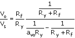
this is the noninverting amplifier. Here we obtain the relationship between the
amplifier gain, avo = Vo/Vs,
and the open-loop gain (opamp gain), avo
= Vo/V![]() , and the circuit resistors.
, and the circuit resistors.
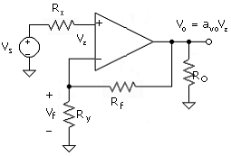
With a signal applied to the plus input terminal, the responding output voltage is fed back to the resistor Ry. The voltage across Ry, Vf, and Vo (signal) are related by
Equation 11.1
![]()
This is just the voltage-divider relation, which applies in this case, as negligible current flows into the input terminals of the opamp. Variable Vf is used in lieu of VRy to distinguish it from the dc value of the voltage across Ry. This use is also consistent with the fact that Vf is technically a signal feedback voltage.
The input signal voltage Vs adds up to
Equation 11.2
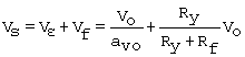
where ( ) is used to eliminate Vf. (The voltage drop across Rx is essentially zero.) This leads directly to the relation for amplifier gain, which is
Equation 11.3
with (ideal noninverting gain).
Equation 11.4
![]()
AvNI
is the limiting form of the noninverting amplifier gain for avo ![]()
![]() . This is consistent with the fact that in the limit, V
. This is consistent with the fact that in the limit, V![]()
![]() 0 and Vs = VRy. Thus, the output and input
voltages are simply related by the voltage-divider relation. The result, ( ), indicates that for avo>>AvNI,
the voltage gain can simply be expressed in terms of the resistors and
therefore is very predictable. If we make, for example, Rf = 10Ry,
AvNI = 11, and ( ) gives Av = 10.998, with
avo = 40,000. The value for the opamp gain is typical for our
project opamp. Note that due to the high resistance at the opamp input
terminals, Rx has no influence on the gain.
0 and Vs = VRy. Thus, the output and input
voltages are simply related by the voltage-divider relation. The result, ( ), indicates that for avo>>AvNI,
the voltage gain can simply be expressed in terms of the resistors and
therefore is very predictable. If we make, for example, Rf = 10Ry,
AvNI = 11, and ( ) gives Av = 10.998, with
avo = 40,000. The value for the opamp gain is typical for our
project opamp. Note that due to the high resistance at the opamp input
terminals, Rx has no influence on the gain.
The noninverting amplifier has a very high input resistance and a low output resistance, as discussed in Unit 11.4. The amplifier technically falls into the category of a series - shunt feedback configuration or a voltage amplifier.
To obtain the inverting amplifier, the signal is applied to the negative or inverting terminal as shown in Fig. 11.4. A positive signal results in a negative output voltage. The gain expression can be obtained with the loop equation from output to input:
Equation 11.5
![]()
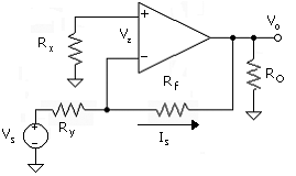
and the loop equation at the input (voltage drop across Rx is zero)
Equation 11.6
![]()
Eliminating Is between ( ) and ( ) gives
Equation 11.7
![]()
This expression can be manipulated to give the gain as
Equation 11.8
which is
Equation 11.9
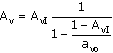
where
Equation 11.10
![]()
AvI is the gain of the ideal inverting amplifier.
The ideal
gain, as in the case of the noninverting amplifier, depends only on resistor
values. The approximate form is based on the approximation V![]()
![]() 0, in which case the negative input terminal is at virtual ground. Thus,
|vo| and Vs are proportional to Rf and Ry,
respectively. The inverting-amplifier gain result includes the fact that the
current into the negative terminal is zero. The circuit is a shunt - shunt feedback configuration or a
transresistance amplifier.
0, in which case the negative input terminal is at virtual ground. Thus,
|vo| and Vs are proportional to Rf and Ry,
respectively. The inverting-amplifier gain result includes the fact that the
current into the negative terminal is zero. The circuit is a shunt - shunt feedback configuration or a
transresistance amplifier.
The negative feedback of the amplifiers will alter the output resistance of the circuit. In the case of series - shunt feedback (noninverting amplifier) and the shunt - shunt (inverting amplifier), the output resistance will be reduced from that of the open-loop amplifier. This can be explained with the use of the circuit of Fig. 11.5, which shows a linear-model circuit for the amplifiers of Figs. 11.3 and , with the inputs set to zero.
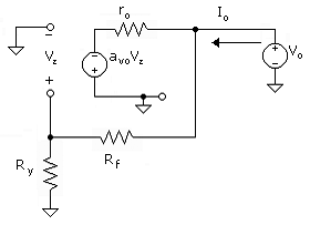
For the present purposes, a voltage-dependent voltage source equivalent circuit for the opamp is chosen. The parameter ro is the output resistance of the open-loop opamp. For example, the output resistance would be about 1/gm in a CMOS opamp with a source-follower stage-output stage.
A test
voltage, Vo, is applied at the output terminal with the input
grounded. This results in an input to the opamp of magnitude V![]() = Vo/AvNI. The
voltage-dependent voltage source of the opamp is thus (avo/AvNI)Vo.
The total current, Io, flowing from the test voltage is then
= Vo/AvNI. The
voltage-dependent voltage source of the opamp is thus (avo/AvNI)Vo.
The total current, Io, flowing from the test voltage is then
Equation 11.11
![]()
Therefore, the output resistance is
Equation 11.12
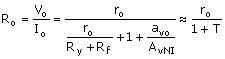
where T = avo/AvNI
(i.e., the loop gain of the feedback
amplifier). The approximate form comes from the expectation that ro
<< Ry + Rf; it neglects the current through the
feedback resistors. Ro ![]() ro/T is a valid approximation in most cases and Ro
<< ro. For example, for AvNI
ro/T is a valid approximation in most cases and Ro
<< ro. For example, for AvNI ![]() 10 and avo
10 and avo ![]() 40,000, T = 4000, and Ro
40,000, T = 4000, and Ro ![]() ro/4000.
ro/4000.
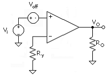
Ideally, an opamp is balanced such that the dc output is zero (with dual power supply) with zero input voltage (as in Fig. 11.1). In practice, this is not realized, due to the variation of parameters between similar transistors and components. As mentioned above, the opamp configuration of Fig. 11.1 will probably be locked at near the positive or negative rail voltage. Thus, a given opamp requires an input voltage Vin to set the output to zero. The magnitude of this voltage is defined as offset voltage Voff.
An equivalent circuit that includes the offset voltage is given in Fig. 11.6. The imperfections of the amplifier are reflected into the offset voltage and the opamp is ideal. If Vi is made equal to Voff, the output VO will be zero. Suppose that Vi = 0. In this case we have the equivalent of Voff applied to the input and the output is driven toward the plus or minus power-supply voltages (depending on the polarity of Voff). Voff is usually large enough to cause the amplifier to be driven out of the active mode. For example, a typical Voff is Voff = 1 mV. Thus, if avo = 40,000, the output will attempt to become -40 V, which is probably greater than the supply voltage value; the output is set at the negative limit. In our project opamp, this will be roughly VSS + 50 mV if driven negative or VDD -1V if driven toward the positive supply.
The dc output voltage can be set close to zero with negative feedback for normal operation as a linear amplifier as illustrated in Fig. 11.7. A portion of the output voltage is applied back to the input as the voltage across Ry. This is
Equation 11.13
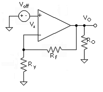
(Dc VO is used, as this is a no-signal or bias state under consideration.) This voltage will cancel most of Voff, such as to drive VO close to zero if Rf is small enough compared to Ry. The value of VO for a given Rf can be obtained as follows: A loop equation at the input side (Fig. 11.7) gives
Equation 11.14
![]()
The opamp
circuit is a dc amplifier. Therefore, the input - output relation holds for dc
as well as for signals. Thus, V![]() = VO/avo such
that
= VO/avo such
that
Equation 11.15
![]()
and
Equation 11.16
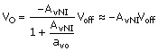
where the
approximation usually applies and is equivalent to V![]()
For example,
with Voff = 1 mV and AvNI = 100, Vo ![]() -0.1 V. This would be a very satisfactory dc state for using the circuit
as an amplifier. Also, the approximation of the right-hand side of ( ) is quite valid. Note that without
the feedback network, VO = -avoVoff = -40,000
· 1 mV = -40 V. Assuming that the power-supply voltage is, for example, ±15 V,
the output is locked at VO
-0.1 V. This would be a very satisfactory dc state for using the circuit
as an amplifier. Also, the approximation of the right-hand side of ( ) is quite valid. Note that without
the feedback network, VO = -avoVoff = -40,000
· 1 mV = -40 V. Assuming that the power-supply voltage is, for example, ±15 V,
the output is locked at VO ![]() -15 V and the linear gain relation does not apply. In our project with
the opamp, we determine Voff from a measurement of VO and
the application of (
-15 V and the linear gain relation does not apply. In our project with
the opamp, we determine Voff from a measurement of VO and
the application of (
The MOSFET has a number of capacitances, including those associated with the gate structure and source and drain pn junctions as well as other parasitic capacitors of the transistor and the circuit. Therefore, the open-loop opamp will tend to be unstable due to the poles and zeros associated with the capacitors. Opamps are usually stabilized with the addition of a capacitor. The added pole is well below the lowest naturally occurring pole. This pole will dominate the frequency response of the opamp. In a lab project, the pole frequency will be measured.
We will obtain the frequency response of the feedback amplifier based on the single-pole response. The form of the response of the open-loop opamp is
Equation 11.17
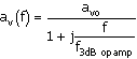
The response
function has value avo at low frequencies and has magnitude ![]() at f = f3dB opamp, where
f3dB opamp is the characteristic frequency of the opamp. This is
indirectly, f3dB opamp = GBP/avo, where GBP is the gain -
bandwidth product of the opamp as given in the datasheet. Datasheet value avo
is also given (Avd, large-signal voltage gain).
at f = f3dB opamp, where
f3dB opamp is the characteristic frequency of the opamp. This is
indirectly, f3dB opamp = GBP/avo, where GBP is the gain -
bandwidth product of the opamp as given in the datasheet. Datasheet value avo
is also given (Avd, large-signal voltage gain).
The noninverting feedback amplifier has a gain as given by ( ). That expression is used here along with ( ) in place of avo. The frequency response of the feedback amplifier is thus
Equation 11.18
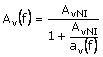
which is
Equation 11.19
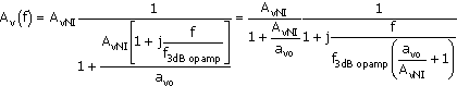
This can be simplified to
Equation 11.20
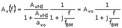
where Avo is the amplifier gain at low frequencies and where
Equation 11.21
![]()
Frequency parameter fBW is the bandwidth of the amplifier for a specific AvNI · Parameter fBW, by definition of bandwidth, is also f3dB of the amplifier. Adding feedback by reducing Rf always increases bandwidth at the expense of gain. Note that for Rf very small, fBW can be relatively high and the frequency response is complicated by the fact that other poles of the opamp come into play.
Given in Table 11.1 is a segment from the manufacturer's datasheet for the opamp (TS271C) used in our project. As mentioned above, the parameter for large-signal voltage gain is designated as Avd and is identical to avo. The GBP indicated is 700 kHz. Thus for a low-frequency amplifier gain of, for example, Av = 5000, the bandwidth is fBW = 700 kHz/5K = 140 Hz, which can be readily measured using LabVIEW and the DAQ in the computer.
|
TABLE 11.1 |
|||||
|
Symbol |
Parameter |
TS271C/AC/BC |
Unit |
||
|
Min. |
Typ. |
Max |
|||
|
Avd |
Large Signal Voltage Gain VO = 1 V to 6 V, RL = 100 kW, Vic = 5 V Tmin. < Tamb < Tmax. |
V/mV |
|||
|
GBP |
Gain Bandwidth Product (Av = 40dB, RL = 100 KW, CL = 100pF, fin = 100 KHz) |
MHz |
|||
Note that for
the limiting case of Rf ![]()
![]() , the bandwidth of the open-loop amplifier is only f3dB = 700
kHz/50K = 14 Hz, where the typical (Typ.) number, Avd = 50 k has
been used.
, the bandwidth of the open-loop amplifier is only f3dB = 700
kHz/50K = 14 Hz, where the typical (Typ.) number, Avd = 50 k has
been used.
|
|
Noninverting feedback amplifier voltage gain. |
|
|
Ideal noninverting amplifier voltage gain. |
|
|
Inverting feedback amplifier voltage gain. |
|
|
Ideal inverting amplifier voltage gain. |
|
|
Output resistance of the resistance-feedback opamp amplifier. |
|
T = avo/AvNI |
Loop gain of resistance-feedback opamp amplifier. |
|
|
Output voltage of resistance-feedback opamp with offset voltage, Voff. |
|
|
Frequency-response function of resistance-feedback opamp amplifier. |
|
|
Bandwidth (corner frequency) of opamp amplifier with opamp open-loop corner frequency, f3dB. |
|
Project Mathcad Files |
Exercise11.mcd - Project11.mcd |
|
Laboratory Project 11 |
Operational Amplifier with Resistor Feedback |
|
P11.2 |
Bias Circuit Setup |
|
P11.3 |
Opamp Offset Voltage |
|
P11.4 |
Evaluation of the Bias Balancing Circuit |
|
P11.5 |
Evaluation of the Gain and Signal Limits with Swept Input |
|
P11.6 |
Evaluation of the Gain with Sine-Wave and Square-Wave Signals |
|
P11.7 |
Determination of the Opamp Frequency Response |
|