The basic low-frequency linear model for a MOS transistor has three conductance parameters: the transconductance parameter, gm, the body-effect parameter, gmb, and the output conductance parameter gds. They are the proportionality constants between incremental variables of current and voltage. For the linear model to be valid, the increment must be small compared to the dc (bias) value of the variable. To qualify as small, the increment must be sufficiently small, in each case, as to avoid unacceptable degrees of nonlinearity in the variable relationships. The conditions are explored in Unit 5 in connection with linearity of an amplifier gain function.
In the following, the three conductance parameters are explored, and in each case, an expression for obtaining the circuit value is developed. The discussion is based on a standard amplifier stage to provide for an association with electronic circuits.
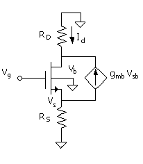
To serve as an illustration of the utility of the parameters, the discussion of the linear model and g parameters will be accompanied by a signal-performance evaluation of an NMOS transistor in the most general amplifier configuration (Fig. 4.1). The circuit includes drain and source resistors, and input is at the gate terminal. As shown in Fig. 4.1(b), output can be at the drain (common-source amplifier) or 17217h79r source (source-follower amplifier).
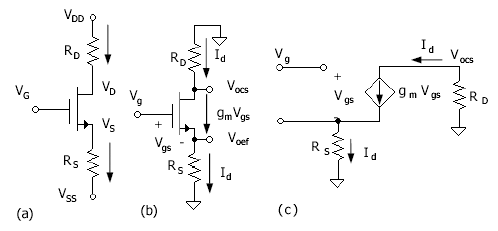
Figure 4.1 shows the dc (bias) circuit (a) and signal circuit (b). Replacing all dc nodes with signal ground and replacing the dc variables with signal variables as in Fig. 4.1 produces the signal circuit. It will be assumed that the schematic symbol for the transistor in signal circuit (b) is equivalent to the ideal, intrinsic linear model of the transistor. The total drain current of the model is Id = gmVgs, as, for example, in the basic circuit of Fig. 2.4. The linear equivalent model is that of Fig. 4.1(c). The symbolic transistor in Fig. 4.1(b) is more intuitively representative in terms of the overall circuit perspective than that of Fig. 4.1(c). For this reason, the Fig. 4.1(b) version is chosen for use in all of the following discussions of MOSFET circuits. All other details of the transistor model, as discussed in this unit, will be added externally.
Signal Vg = Vi is applied to the gate (input) and, in response, a signal voltage, Vo, appears at the drain (or source). We would like to analyze the signal performance in terms of voltage gain, av = Vo/Vi = Vd/Vg (or av = Vs/Vg), of the circuit based on a linear (small-signal) analysis. In any case, the voltage gain is av = GmRx, where Gm is the circuit transconductance (as opposed to the transistor transconductance) and x = D (common source) or x = S (source follower). Thus, the goal will be to obtain a relation for Gm for a given linear model of the transistor. Circuit transconductance is determined in the following for models with the various parameters included.
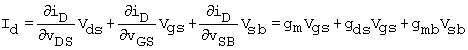
As illustrated previously diagrammatically, for example, in Fig. 3.2, the MOSFET is a four-terminal device. The four-terminal version of the schematic symbol is repeated here in Fig. 4.2. The terminals again are the source, drain, gate, and body. The drain current and the three terminal-pair voltages are all interdependent such that iD = f(vDS, vGS, vSB). Use of the three-terminal schematic symbol for the transistor, as in Fig. 4.1, conveys the assumption that the body and source are connected. For an applied incremental Vgs, for example, there will be, in response, incremental drain current Id and incremental voltages Vds and Vsb. The linear model is based on relating the current to the three voltages. This is
Equation 4.1
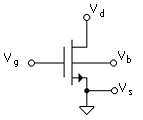
The linear-model representation is shown in Fig. 4.3 Figure 4.3(a) shows a current-source version. The body-effect parameter, gmb, is defined as positive. The minus sign is required as the partial derivative in ( ) is negative. In Fig. 4.3(b) the body-effect current source is reversed to eliminate the minus sign, and the current source associated with gds is replaced with a resistance. The latter is possible as the voltage-dependent current source is between the same nodes as the voltage.
In the following units, using the detailed functions ( ) and ( ), which relate the four variables, expressions, as used in SPICE, will be obtained for the three proportionality constants: transconductance parameter, gm, output conductance parameter, gds, and body-effect transconductance parameter, gmb. The results will be used to obtain numerical results for the circuit transconductance, Gm, for various cases.
The transconductance parameter, gm, was introduced in Unit 2 in the treatment on the rudimentary electronic amplifier; it is the proportionality constant of the linear relationship between the output (responding) current and the input (control) voltage [( )]. For the MOSFET, NMOS, or PMOS, Id = gmVgs, where Id is into the drain for both transistor types. An ideal transistor can be modeled with this alone. A simple model, which includes no other components, would often be adequate for making estimates of circuit performance.
To obtain an expression for gm as a function of the general form iD = f(vGS, vDS, vSB) [e.g., ( )], we use the definition [from (
Equation 4.2
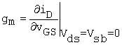
Using ( ) to express iD, the resulting relation for gm is
Equation 4.3
![]()
where ![]() )] and Veffn = VGS
- Vtno. Note that the use of VDS is consistent with the
partial derivative taken with respect to vGS, that is, Vds
= 0. Also, the use of Vtno implies that vSB = 0. In
general, VSB could be nonzero, although in the definition of gm,
Vsb must be zero. For the case of nonzero VSB (bias), one
substitutes for Vtno a constant Vtn(VSB) in
the gm expression.
)] and Veffn = VGS
- Vtno. Note that the use of VDS is consistent with the
partial derivative taken with respect to vGS, that is, Vds
= 0. Also, the use of Vtno implies that vSB = 0. In
general, VSB could be nonzero, although in the definition of gm,
Vsb must be zero. For the case of nonzero VSB (bias), one
substitutes for Vtno a constant Vtn(VSB) in
the gm expression.
Alternative forms for the gm expression can be obtained from ( ), which is, solving for Veffn,
Equation 4.4
![]()
Using ( ), and ( ), gm takes on altogether three forms:
Equation 4.5
![]()
Usually, in
initial design, kn replaces ![]() to eliminate the VDS
dependence without a serious penalty in accuracy.
to eliminate the VDS
dependence without a serious penalty in accuracy.
Using the simple linear transistor model, an expression for the circuit transconductance, Gm, for the circuit of Fig. 4.1 will now be obtained. The input loop equation for an applied gate signal voltage, Vg, is
Equation 4.6
![]()
which is, with Vgs = Id/gm,
Equation 4.7
![]()
and
Equation 4.8
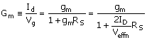
The far right-hand side uses ( ). For example, for a 1-V drop across RS and Veffn = 0.5 V, Gm = gm/5. Note that the ratio of the signal voltage drop across RS and signal voltage Vgs is gmRS:1. The Gm concept is utilized routinely in MOSFET circuits (and BJT circuits), which gives the effective reduced transconductance, referred to Vg, in the presence of the source resistor.
For circuits in which the signal Vsb is nonzero, there will be an additional component of Id, gmbVsb. An example is the circuit of Fig. 4.1 but with body terminal connected to ground. This feature is added to the circuit as shown in Fig. 4.4. The proportionality constant for this case, gmb, is the body-effect transconductance. It is defined as
Equation 4.9
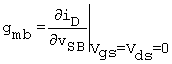
which is [with ( ) and ( ) for iD and Vtn]
Equation 4.10
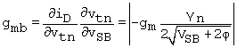
The minus sign is consistent with a current source in the opposite direction from that of Fig. 4.4 (as shown in Fig. 4.3) as iD is defined as positive into the drain. The preference is to turn the current source around as in Figs. 4.3 and and use positive gmb. The result for gmb is a factor, h, times gm, that is
Equation 4.11
![]()
For gn = 0.5 V1/2, VSB = 5 V,
and 2FF = 0.7 V, gmb = 0.1gm (h = 0.1). Note that gmb is not
zero even with the source connected to the body [i.e., with VSB = 0
in ( )]. However, signal Vsb
is zero in such a case, such that gmb does not have to be taken into
account. In general, even with VSB ![]() 0 it is possible for Vsb
0 it is possible for Vsb ![]() 0, in which case, gmb must be included in the model (e.g., in
Project
8 on
the study of the source-follower stage, at the low end of the bias current
scan).
0, in which case, gmb must be included in the model (e.g., in
Project
8 on
the study of the source-follower stage, at the low end of the bias current
scan).
The output conductance accounts for the finite slope of the output characteristic, an example of which is shown in Fig. 4.5. The plot for the SPICE formulation [( )] of the active region is also shown (applicable to the device for VDS > Veffn). Both plots are for VGS = constant (i.e., Vgs = 0 and gmVgs = 0).
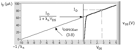
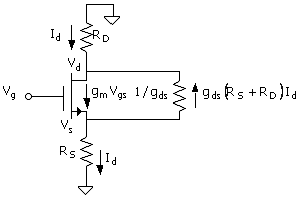
In the ideal case, for any vDS in the active region, the current is the same for a given VGS, and the drain current is simply Id = gmVgs. The real case, though, obviously possesses a current dependence on vDS. The linear model treats gm as a constant (calculated at the bias values) and includes the effect of the nonzero slope with the output conductance, gds, such that Id = gmVgs + gdsVds (without or neglecting the body effect). The circuit shown in Fig. 4.6 includes the gds component.
An expression for the output conductance is obtained from the definition
Equation 4.12
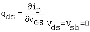
Again using ( ), the result is
Equation 4.13
![]()
where Veffn = VGS - Vtno is constant and where ID is the dc (bias) current. The last term (on the right-hand side) is the form that is generally used in practice for an initial design, as it does not require a value for VDS. Note that gds is not a conductance in the physical sense but has the correct dimensions and behaves in the circuit like a conductance.
We will now obtain the circuit transconductance for the case where the effect of gds is included. Upon application of an input signal, Vg, a signal drain current, Id, will flow in the output circuit. This causes a signal voltage to appear across RS and RD, which is equal to the voltage to Vds. That is,
Equation 4.14
![]()
The associated current through the output resistance is thus
Equation 4.15
![]()
The effect is to reduce the current through RS and RD and thus reduce the circuit transconductance of the common-source amplifier stage. The output current with the current of ( ) subtracted from the basic gmVgs is
Equation 4.16
![]()
which is, when solved for Vgs,
Equation 4.17
![]()
Again using ( ), which is Vg = Vgs + IdRS, the new circuit transconductance is
Equation 4.18
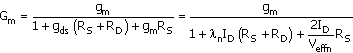
With a 1 - V drop across RS and a 5 - V drop across RD, and with ln = 1/50 V, the new Gm is gm/5.12, compared with gm/5 when neglecting gds [(
In general, the complete circuit includes, in addition, the body-effect transconductance current source of Figs. 4.3 and . The omission of this current source in Fig. 4.6 implies that Vsb = 0 because the source and body are connected. This connection is possible to implement in special cases such as in some of our MOSFET lab projects where only one transistor on the chip is used or for the case of a differential stage where the source of two transistors is at the same node. It is also possible to eliminate the body-effect current source by bypassing the source resistor with a bypass capacitor. The capacitor places the source at signal ground. However, in this case, the dc threshold voltage is still affected by VSB = IDRS.
In Unit 8, the circuit transconductance equivalent to ( ) and ( ), but which includes the body effect [( )], is given as
![]()
where h is defined in ( ). For gds = 0 and h ) reduces to ( ). Note that including the body effect will in general have more effect on Gm than including gds, as h can be on the order of 0.2. In all cases where we can calculate the circuit transconductance, Gm, the magnitude of the voltage gain is obtainable from -GmRD (common-source stage) and GmRS(source-follower stage).
The transistor output characteristics from Unit 3 and the variable increments along with their linear relationships are illustrated in Fig. 4.7. This would be applicable, for example, to the amplifier of Fig. 2.4. (As in that circuit, no body effect is included.) The circuit is biased with drain - source voltage VDS and drain current ID. A positive signal Vg is applied to the gate terminal. In response, there appears drain signal voltage -Vd, due to the rise in drain current. Signal voltages are with respect to the source or ground.
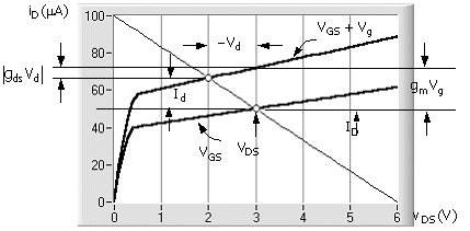
The two output characteristic curves correspond to bias VGS only and with gate voltage VGS + Vg. In both cases, the solution to the drain current and voltage is the intersection between the transistor characteristic curve and the load line, which is a plot of the output circuit loop equation. This is (with reference, for example, to Fig. 2.4)
Equation 4.19
![]()
The solution is always constrained to this straight-line equation. The solution for vDS with and without signal is based on ( ) and ( ), which is
![]()
The combined contributions to Id associated with the two g parameters is
Equation 4.20
![]()
By the nature of the load-line function, the two terms will always have opposite signs; when Vg is negative, Vd will be positive.
|
where
|
Transconductance. |
|
where
|
Approximate transconductance. |
|
|
Amplifier circuit transconductance with a source resistance. |
|
|
Body-effect transconductance. |
|
|
Output conductance. |
|
gds = lnID |
Approximate output conductance. |
|
|
Amplifier circuit transconductance with gds included. |
|
Subscripts are for NMOS. All equations are the same for PMOS with "p" subscript substitution and subscript-order reversal for bias-voltage variables. |
|
|
