UNIVERSITY POLITEHNICA OF
FACULTY OF ENGINEERING IN MODERN LANGUAGE
EVOLVBLE INTERNET HARDWERE PLATFORMS
-Field Programmable Gate Array-
Constantin Stanciu
FILS 1242 EE
Electronics design
The invention of the transistor has changed not only the electronics industry but the whole world because of its size speed and design simplicity. Transistor circuits are used in many circuits starting from amplifiers up to musical instruments circuits.
The transistors are used as switches to turn circuits on and off. This phenomenon helped in the design of many circuits such as alarms, control circuits and all circuits that are based on on-off technique.
Digital design makes use of this on-off that is symbolized by 1-0. These 0s and 1s are the basics of the Boolean arithmetic.
Digital design
Digital design makes use of the Boolean functions to implement its circuits. AND, OR, NOT are the basic functions that can generate all other functions. All Arithmetic and logic functions can be implemented using these functions.
Besides that, Flip-flops and registers are used in digital design to implement memory or storage element in the design, so the circuit can remember its old state to calculate the new state and act accordingly.
There are two types of digital circuits synchronous (Clocked) and asynchronous (non-clocked) circuits.
Advantages of digital design:
LIBRARY ieee;
USE ieee.std_logic_1164.ALL;
ENTITY Adder_ent IS
PORT (
Op1 : IN std_logic; -- Operand 1
op2 : IN std_logic; -- Operand 2
carry : OUT std_logic; -- Output carry
Result : OUT std_logic); -- Result
END Adder_ent;
ARCHITECTURE behavior OF Adder_ent IS
BEGIN -- behavior
Result <= (Op1 AND NOT Op2) OR (NOT Op1 AND Op2);
Carry <= Op1 AND Op2;
END behavior;
A prototype platform has been developed that allows processing of packets at the edge of a multi-gigabit-per-second network switch. This system, the Field Programmable Port Extender (FPX), enables packet processing functions to be implemented as modular components in reprogrammable hardware. All logic on the on the FPX is implemented in two Field Programmable Gate Arrays (FPGAs). Packet processing functions in the system are implemented as dynamically loadable modules.
Core functionality of the FPX is implemented on an FPGA called the Networking Interface Device (NID). The NID contains the logic to transmit and receive packets over a network, dynamically reprogram hardware modules, and route individual traffic flows. A full, non-blocking, switch is implemented on the NID to route packets between the networking interfaces and the modular components. Modular components of the FPX are implemented on a second FPGA called the Reprogrammable Application Device (RAD).
Modules are loaded onto the RAD via reconfguration and/or partial partial reconfguration of the FPGA. Through the combination of the NID and the RAD, the FPX can individually reconfigure the packet processing functionality for one set of track flows, while the rest of the system continues to operate. The platform simplyst the
development and deployment of new hardware-accelerated packet processing circuits.
The modular nature of the system allows an active router to migrate functionality from
software pluggins to hardware modules.
The
Components of the FPX include two FPGAs have banks of memory, and two high-speed network interfaces. Networking interfaces on the FPX were optimized to enable the
simultaneous arrival and departure of data cells at SONET OC48 rates. This is the equivalent bandwidth of multiple channels of Gigabit Ethernet.
The FPX implements all logic using two FPGA devices: the Network Interface Device (NID) and the Reprogrammable Application Device (RAD).
The RAD contains the modules that implement the module-specific functionality. Each module on the RAD connects to one Static Random Access Memory (SRAM) and
to one, wide Synchronous Dynamic RAM (SDRAM). In total, the modules implemented on the RAD have full control over four independent banks of memory.
The SRAM is typically used for applications that need to implement table lookup operations (like the Fast IP lookup algorithm), while the SDRAM interface is typically used for applications like packet queuing that transfer bursts of data and can tolerate a higher memory latency.
The RAD communicates with the NID using a Utopia-like interface. Packets on this interface are segmented into a sequence of fixed-size cells that are formatted as IP over ATM.
Each interface has a small amount of buffering and implements flow control. A Start of Cell (SOC) signal is asserted at the input of a module to indicate the arrival of data.
The Transmit Cell Available (TCA) signal is asserted back towards an incoming data source to indicate downstream congestion.
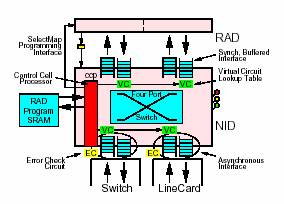
The Network Interface Device (NID) on the FPX controls how packet flows are routed to and from modules. It also provides mechanisms to dynamically load hardware modules
over the network and into the router. The combination of these features allows these modules to be dynamically loaded and unloaded without affecting the switching of other traffic flows or the processing of packets by the other modules in the system.
The NID has several components, all of which are implemented in FPGA hardware. It contains a four-port switch to transfer data between ports; Virtual Circuit lookup tables (VC) on each port in order to selectively route flows; a Control Cell Processor (CP), which is used to process control cells that are transmitted and received over the network; logic to reprogram the FPGA hardware on the RAD; and synchronous and asynchronous
interfaces to the four network ports that surround the NID
The NID routes flows among the modules on the RAD and the network interfaces to the switch and line card using a four-port switch.
Each traffic flow that arrives on any incoming port can be forwarded to any destination port.
Each of the NID's four interfaces provide a small amount of buffering for short-term congestion. Buffers on the NID are implemented using on-chip memory. When packets contend for transmission to the same destination port, the NID performs arbitration. For longer term congestion, the NID avoids data loss by sending a back-pressure signal to the previous module or network interface along the that network flow's path.
The design of the four-port switch and scheduling algorithm used to arbitrate among flows is based on the design of the iPOINT switch .
IP Packets are routed through the FPX and switch based on assignment of cell headers that transport that packet.
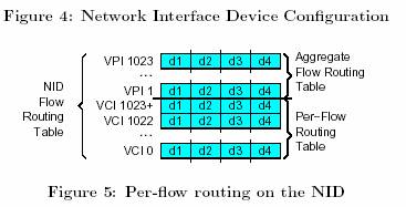
The NID supports forwarding for both aggregate traffic flows and individual traffic flows. The NID's Virtual Circuit look up table (VC) maps these flows into next-hop destinations at each of the four ports.
The NID's flow routing table contains entries for each of the four ports in the switch that identify the destination port of each flow. The table has sufficient entries to support 1024 virtual paths for aggregated traffic and another 1024 virtual circuits for individual flows.
To implement egress flow processing (i.e., process packets as they exit the router), the NID routes a flow from the switch, to a RAD module, then out to the line card. Likewise, to implement ingress cell processing, the NID routes a virtual circuit from the line card, to a RAD module, then out to the switch. Full RAD processing occurs when data is processed in both directions by both modules on the RAD. Loopback and partial loopback testing can be programmed on the NID to debug experimental modules. Modules can implement selective packet forwarding by reassignment of the headers
that transport each packet.
The NID implements a Control Cell Processor (CCP) in hardware to manage the operation of the FPX and to communicate over the network. On the ingress interface from the switch, the CCP listens and responds to commands that are sent on a specific virtual circuit. The NID processes commands that include: (1) modification of per-flow routing entries; reading and writing of hardware status registers, reading and writing of configuration memory, and commands that cause the logic on the RAD to be repro-
grammed. After executing each command, the NID returns a response in a control cell.
When we talk about reconfigurable computing we're usually talking about FPGA-based system designs. Unfortunately, that doesn't qualify the term precisely enough. System designers use FPGAs in many different ways.
The most common use of an FPGA is for prototyping the design of an ASIC. In this scenario, the FPGA is present only on the prototype hardware and is replaced by the corresponding ASIC in the final production system. This use of FPGAs has nothing to do with reconfigurable computing.
However, many system designers are choosing to leave the FPGAs as part of the production hardware.
The logic within the FPGA can be changed if or when it is necessary, which has many advantages. For example, hardware bug fixes and upgrades can be administered as easily as their software counterparts. In order to support a new version of a network protocol, you can redesign the internal logic of the FPGA and send the enhancement to the affected customers by email. Once they've downloaded the new logic design to the system and restarted it, they'll be able to use the new version of the protocol. This is configurable computing; reconfigurable computing goes one step further.
Reconfigurable computing involves manipulation of the logic within the FPGA at run-time. In other words, the design of the hardware may change in response to the demands placed upon the system while it is running. Here, the FPGA acts as an execution engine for a variety of different hardware functions - some executing in parallel, others in serial - much as a CPU acts as an execution engine for a variety of software threads. We might even go so far as to call the FPGA a reconfigurable processing unit (RPU).
Reconfigurable computing allows system designers to execute more hardware than they have gates to fit, which works especially well when there are parts of the hardware that are occasionally idle.
One theoretical application is a smart cellular phone that supports multiple communication and data protocols, though just one a time. When the phone passes from a geographic region that is served by one protocol into a region that is served by another, the hardware is automatically reconfigured. This is reconfigurable computing at its best, and using this approach it is possible to design systems that do more, cost less, and have shorter design and implementation cycles.
Technical advantages Reconfigurable computing has several advantages. First, it is possible to achieve greater functionality with a simpler hardware design. Because not all of the logic must be present in the FPGA at all times, the cost of supporting additional features is reduced to the cost of the memory required to store the logic design.
Consider again the multiprotocol
cellular phone. It would be possible to support as many protocols as could be
fit into the available on-board
The second advantage is lower system cost, which does not manifest itself exactly as you might expect. On a low-volume product, there will be some production cost savings, which result from the elimination of the expense of ASIC design and fabrication. However, for higher-volume products, the production cost of fixed hardware may actually be lower.
The final advantage of reconfigurable computing is reduced time-to-market. The fact that you're no longer using an ASIC is a big help in this respect. There are no chip design and prototyping cycles, which eliminates a large amount of development effort. This allows an incremental design flow, a luxury not typically available to hardware designers.
Traditional FPGAs are configurable, but not run-time reconfigurable. Many of the older FPGAs expect to read their configuration out of a serial EEPROM, one bit at a time. And they can only be made to do so by asserting a chip reset signal. This means that the FPGA must be reprogrammed in its entirety and that its previous internal state cannot be captured beforehand. Though these features are compatible with configurable computing applications, they are not sufficient for reconfigurable computing.
In order to benefit from run-time reconfiguration, it is necessary that the FPGAs involved have some or all of the following features. The more of these features they have, the more flexible can be the system design.
Whenever possible, we'd like to avoid resetting the FPGA, mostly because it takes a lot of time. Ideally, we could just stop the clock going to some or all of the chip, change the logic within that region, and restart the clock. That way, there isn't as much wasted time, or configuration overhead. The more configuration overhead there is the more likely that the system performance will be unacceptably below that of a fixed-hardware version.
Partial reprogrammability
Even better would be the ability to leave most of the internal logic in place and change just one part. The Atmel 40K and Xilinx 62xx series FPGAs have such a feature. Any gate or set of gates may be changed without affecting the state of the others. It will always be much faster to change a small piece of the logic than the entire FPGA contents.
The Internet is a platform? Yes, the combination of browsers, HTML, scripting languages, Java, and all the web servers out there is a huge platform. And, as computers get cheaper, and web-top-boxes like WebTV spread and increase their capabilities, this platform has a good chance of spreading into most of the homes in the world. The key is that all the open technologies of the Internet work on all the computers in peoples homes and offices. Instead of talking about a market made up of 25% or even 66% of computers, we are talking about a market made up of 100% of computers, a growing number of web-top-boxes, and soon millions of new and existing cable TV set top boxes. Game developers must pay attention to this platform.
|
