ALTE DOCUMENTE
|
||||||||||
Logic 3.0 for Windows Demo Tutorials
This tutorial is for use with the Demo version of B2 Logic 3.0 and should give you adequate information on the use of the program. The entire version of the manual is available when you order the program.
Ordering information:
Beige Bag Software
279 E. Liberty
Ann Arbor, MI 48104
Phone (734) 332-0487 Fax (734) 332-0392
Email: orders@beigebag.com
Internet: https://www.beigebag.com
Tutorial #1
Build a three input And function
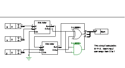
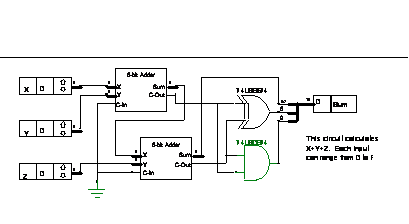
During this tutorial, you will build a three input And function out of a three input Nand gate (7410) and an Inverter (7404). A picture of the final circuit is shown below.

Open the B Logic program
Choose New from the File menu to bring up a clean circuit window.
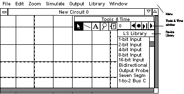
The selection arrow should be the active tool and cursor. It's the active tool because its icon is inverted in the tool bar. The 0 ns displayed with the simulation controls represents the current simulation time. It is zero because you have not told B Logic to start simulating the circuit yet. Just to get a hang of the interface, try moving the device library around by dragging its title bar. You can resize it by dragging the edges and corner. You can also move the Tools and Time window around, but it can't be resized. The circuit window itself can also be moved and resized.
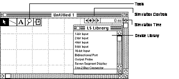
If the device library is not showing, then check to see if there are any libraries available in the Library menu. If there aren't any, then choose Load Library from the Library menu and find the LS library. It should be in the Libraries directory in the program directory. It's named ls.lib.
If a library other than the LS library is active, then choose the LS library from the Library menu to make the LS library active. If the LS library is not in the Library menu, then load the LS library as described above.
Insert an Input
Click on the 1-bit Input in the device library (W double click if you're using MS Windows), then move the cursor into the circuit area. The ghost image of the input port will be following the arrow. Click the mouse button to place down the input port. To deselect the input port, click anywhere else in the circuit area.
To get a feel for the program, click in the input port again. If you click on the name or value of the input port, you can drag it around the circuit. Click on the up and down arrows to change its value.
If you click on the end point of the pin sticking out of the input, you can drag a wire out from the pin. To delete the wire, first select it by double clicking on the wire, then depress the Delete key, or choose Clear from the Edit Menu. See the section on deleting wires if you need more help.
Add two more Inputs
If the input port isn't selected (it'll have a dotted outline or be colored red if it's selected), then click on its name once to select it. Choose Copy from the Edit menu. Then choose Paste from the Edit menu. Place the new 1-bit Input below the first. Choose Paste from the Edit menu again, and place the third 1-bit input below the second. See figure 1.
Insert a three-input Nand gate
The LS library should be the active library. If it isn't then choose it from the Library menu. If it isn't in the Library menu, then load it from the disk. Choose the 'LS10/3 3-input Nand from the device library. Place the nand gate to the right of the three input ports. See figure 2.

Draw the first wire
Click on the line drawing tool (the one that looks like "\") in the toolbox. The cursor will change into a crosshair. Now you can draw the wires.
Click at the rightmost end of the output pin of the top input port. Release the mouse button and move the mouse, and the wire will follow the cursor. Move to the location where you want the first segment of the wire to end, and click once there. Continue drawing segments until you reach the left end of the top input pin of the Nand gate, then double click. The first wire should now be complete. If there is still a wire following the cursor around, use the right mouse button to end the wire.
You will know that the wire has made connections because there will be small squares indicating points where a wire meets a pin. These small squares also are used when three or more line segments intersect at a single point.
Now repeat the process for the second and third pins of the input port to the second and third pins of the Nand gate. See figure 2.
Place and connect the Inverter
Select the arrow, or selection tool, from the toolbox. Then choose the 'LS04/6 Inverter from the device library, and place it to the right of the 3-input nand. Draw a wire connecting the output pin of the 3-input nand gate to the input of the inverter, using the method you learned in step 5. See figure 3.
Place and connect an output probe
Select the Output Probe from the device library.
Rename the inputs and outputs
The circuit is now functionally complete. Double click on the top input port where it says In0 and a dialog box will appear asking for the name and value. Enter A for the name, and then click on OK to close the dialog box. Then double click on the second input port where it says In1 and name it B. Repeat the procedure to change the name of the third input to C, and to rename the output from Out0 to Q. See figure 4.
Test the Circuit
If the cursor is not the selection arrow, then choose the Selection Tool by selecting the arrow from the toolbox. Choose Step from the Simulate Menu or click on the third simulation control from the left, the one with the triangle pointing to the right with the large black vertical bar next to it. The simulation time will increase to 20ns, and the output's value will change to 1. Now set the value of the inputs to one by clicking on the up arrow of each input. Using the probe tool, the rightmost tool in the toolbox, you can probe the value and strength of any wire in the circuit. Simply position the left end of the probe tool on the wire, and depress the mouse button.
Choose Step from the Simulate Menu again. The simulation time will increase to 40ns, and the output value will change to 0. Notice that you have to actually force the simulation time to proceed in order to get results from the simulator. This is very different from the lab, where time proceeds automatically and results seem to show up instantaneously.

Save the Circuit
Now choose Save from the File menu. Since the circuit does not have a name yet, the computer will prompt you to name the circuit. Name it, then you can quit and take a break. Congratulations! You have built a 3-input And function, similar to the 74LS11.
Tutorial #2
Build a hierarchical circuit
This tutorial will help you learn how to use buses (grouped wires), user-defined subcircuits, the trace window, and command files. The final circuit will be capable of calculating X+Y+Z, where X, Y, and Z can range from 0 to FF in hexadecimal (255 in decimal).
The component titled 8-bit Adder, which is used twice in the following circuit, is a User-Defined Circuit. The first part of this tutorial involves the design of the 8-bit Adder component. The second part will involve the design of the 3-way Adder shown in the following figure. If you don't want to spend the time on the first part of the tutorial, the result of the first part can be found in the file Adder2x8., and you can go on to Part II.
Part I Design of the 8-bit Adder.
You should already be familiar with drawing wires, placing components, and naming inputs and outputs. If you aren't, then you should go through tutorial number 1.

Place and rename the inputs
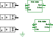
Place and rename the inputs as shown below. If you have a small screen, you'll probably want to choose Zoom Out 1.5 from the Zoom menu. Actually, this is a good time to play around with the zoom features. You can get a close up view of the circuit by choosing Zoom In 1.5 from the Zoom menu, or by choosing the magnifying glass cursor from the toolbar and then clicking on the circuit where you want to zoom in on it. To pan out from the circuit, choose Zoom Out from the Zoom menu, or choose the magnifying glass cursor, then hold down the Ctrl. X and Y are 8-bit Inputs, and C-in is a 1-bit Input. Make sure that an 8 appears above the pin on X and Y. If it doesn't, then double click on the X and Y input ports, and the resulting dialog box will allow you to set the number of bits to 8.
Place a 4-bit Adder and Bus Connectors
This is what the circuit will look like after you finish this step.

The 7483 A chip, a 4-bit adder, is found in the Standard library. If the Standard library is not the active device library, then choose the Standard library from the Library menu. The bus connectors hooked to X and Y are both 1-line to 2-line bus connectors. The bus connectors connected to the left of the 7483A are 1-line to 4-line, and the bus-connector connected to the right of the 7483A is a 4-line to 1-line.
Copy and paste the Adder with its connected Bus Connectors
To select the adder with bus connectors, use the selection arrow to drag a rectangle around the adder and its connected bus-connectors. If you missed one or more of the components that you want to copy, then hold down the shift key while you click on them. Then choose Copy, and then choose Paste from the Edit menu. You will now be dragging around a copy of the 7483 with its connected bus-connectors, and you may place it to the right of the other 7483.
Hook up the wires
Use the wire-drawing tool to hook up the circuit as shown in the following figure. Notice that the busses don't have numbers on their pins yet. If you want to see the bus, choose Recalculate Now from the Simulate Menu.

Hook up the output
The Sum output uses a 2-to-1 Bus Connector and an Output Probe to display a 8-bit wide value. Just hook the Sum and C-Out outputs up as shown on the right of the following figure.

Save the circuit
Choose Save from the File menu. The name you save the circuit under will be its default title when it's used as a component in the next part of tutorial II.
Analyze the circuit
If the simulation time is inverted, meaning white on black, then the circuit drawing might not be up to date. Select Recalculate Now from the Simulate Menu if this is the case. Notice that the simulation time is no longer inverted, the lines that contain more than one wire are thick, and output probe values are no longer inverted. Also, if you look at the bus-connectors, you'll notice that the distribution of wires coming into and out of each bus-connector is specified at the pin. For example, if the pin is labeled 4:7, then the fourth through seventh most significant bits of the bus are on that wire. Bit 0 is the least significant bit. Output ports (probes) are also updated so that they show the number of wires coming in on the bus, and so they show the correct value.
Simulate the circuit
Choose Go from the Simulate Menu (or click the right arrow icon in the simulation controls). You can use the selection arrow tool to click in the up and down arrows in the input ports to change the input values. Or double click on the input port's name to open the dialog box which allows you to type values for the ports.
To simulate the circuit from a command file, choose Do Commands... from the Simulate menu. Specify the file titled adder2x8commands in the dialog box.
The file is named add28cmd.txt on the PC disk. The simulation will execute the commands in the file. You can view or change the command file using any word-processor. The contents of this command file follow this paragraph.
Reset
Set X 1A 0
Set Y 7 0
Set C-in 0 0
Go 100
View the timing diagram
After you've tested the adder, choose Show Trace from the Windows menu (Output menu on the PC) to see the timing diagram. The following diagram is a sample trace. Notice that it takes 27 ns for the sum to appear. You can click in the Timing diagram to see the time at any point.

View the results in tabular format
Choose Show Table from the Windows menu (Output menu on the PC). This is what the table results should look like.
Time X Y C-in Sum C-out
1A 7 0 0 0
1A 7 0 11 0
1A 7 0 21 0
Best and worst case analyses
Choose Set Device Delays... from the Simulate menu, and set all of the devices to their minimum propagation delays. Then repeat the simulation by choosing Do Commands... from the Simulate menu. Specify the same command file you used before in the dialog box. This time, you should notice that sum is generated earlier, after only 15 ns, than in the first case. Finally, choose Set Device Delays... from the Simulate menu, and set all of the devices to their maximum propagation delays. Repeat the simulation from the command file, and notice that it takes longer now, 38 ns, for the sum to appear.
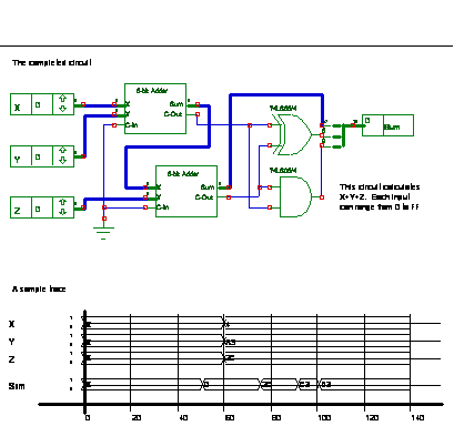
Part II Building the 3-way adder.
In this section you will use the 2-way adder as a completely functional subcircuit in a 3-way adder.
Place the inputs and ground
Select Ground and the inputs from the device list and place it in the circuit window. The inputs are all 8-bit Inputs.
Place the User Defined Circuits
Choose User-Defined Circuit... from the device library. The program will ask you to choose a file. Choose the file that you just built in Part I.
Notice that the inputs and outputs of the new component are ordered according to their vertical location in the 2-input Adder circuit.
To name the subcircuit, double click on it to bring up its dialog box, then enter a name, e.g. 8-bit Adder, in the title field. If you later change the 8-bit Adder, and you want the new 8-bit Adder subcircuit to be used in the 3-way Adder, then you must update the instances of the 8-bit Adder subcircuits using the Update Contents button. Click on OK to exit the dialog box.
Then copy the user-defined circuit and paste another copy below the first.
Complete and simulate the circuit
Hook up the rest of the circuit according to the following picture. The 'LS86/4 Exclusive Or and the 'LS08/4 And gate are both found in the LS Library. To type in the text comment, select the typing tool from the tool palette and click where you want to start the comment, then type the comment in. Then run a simulation on the circuit, a sample trace of which is shown.
Tutorial #3
Build a Ring Counter
This tutorial will illustrate the initial state of the circuit, as well as timing violations.
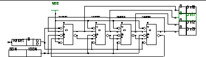
Build or Load the circuit shown above
It is a 4-bit ring counter. The components used are High Voltage (Vcc), 1-bit input, clock, 74LS76 JK flip flop, and the output probe. The 74LS76 flip flop is found in the LS library under the name 'LS76/2 JK Neg Edge Trig FF.
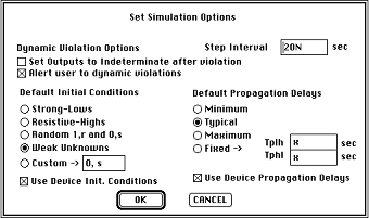
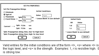
Set the Indeterminate Initial State
Choose Simulation Options from the Simulate Menu. This will bring up the following dialog box. Set the initial conditions to indeterminate (Weak Unknowns). Set the dynamic violation options at the top of the dialog box to notify the user of dynamic violations. Also, check Use Device Initial Conditions, which will allow you to override the unknown initial condition for specific device outputs later in this tutorial.
Run the Circuit
Set the input named Reset to 1, and start stepping the simulation. Notice that the output starts at indeterminate "?" and stays at indeterminate. The output stays indeterminate because the output of each flip-flop feeds into inputs to the flip-flops, forcing the next state of each flip-flop to also be indeterminate.
To get out of the indeterminate state, set Reset to 0, leave it at zero until the outputs clear out to 0, and then bring Reset back up to 1 to allow the simulation to proceed.
More on Initial States
Choose Simulation Options again from the Simulate Menu, but this time set the initial conditions to Resistive High. Then close the Simulation Options dialog, reset the simulation time, set the Reset input to high, and run the simulation again. This time, notice that the simulation starts with all of the outputs at 1, and then goes to all of the outputs at 0, and stays that way until the reset input is set to 0.
By double clicking on an output pin of a flip-flop, you can set the initial state of that individual pin. By double clicking on the flip flop itself, and then clicking on the button called Set Initial State, you can set the initial states of all of the pins of that flip flop.
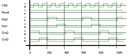
You might want to play around with the initial state, and try different combinations to see what happens to the ring counter. For example, a timing diagram follows that resulted from the initial conditions set to zero for all pins except for the top output of the third flip flop, i.e. the pin connected to the output probe Out2, which has an initial condition of 1,s.
Timing violations
Double click on the clock device in the circuit, and set the clock period and pulse width to 30n and 15n, respectively. Then proceed with the simulation. Notice that as time proceeds, the program alerts you of maximum clock frequency violations. This is because the clock frequency is 33 MHz, and the maximum frequency allowed for the 74LS76 is about 25MHz. When the program alerts you of the error, click on the Stopbutton to make the simulation stop.
Tutorial #4
Customizing Models in B2 Logic
In this tutorial, you will add a 74HC42 model in the Advanced CMOS library in B Logic. Why would you want to do this? Let's say that your parts supplier recently added this part to their catalog, and you want to use it in your design. If you had an HC parts library, you could add it into that library, but since you don't, you can add it to the Advanced CMOS library. If you were planning to use other HC parts also, you would probably want to create a new library of HC parts.
Edit the Advanced CMOS Library.
Select the Advanced CMOS library from the library menu.
If it's not available, then try to load the library using the Load Library menu option. The advanced CMOS library is named ADVCMOST.LIB on the PC platform. After the Advanced CMOS library is active, choose Edit Library from the Library menu.
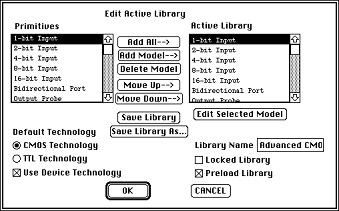
Select the item in the primitive list named '42 BCD to decimal decod. by clicking on it (you may have to scroll down the list to get there). Then click on the Add Model button, and the 7442 will be inserted into the library just before the selected item in the Active Library list.
Edit the model.
Click on the Edit Selected Model button below the library list. This will bring up a dialog box to edit the properties of the 7442 model.
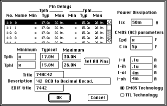
Change the title to 74HC42, and the EDIF title to LS42. Then set the rise times and fall times according to the values shown in the preceding figure. A value of X means unspecified. In general a device's propagation delay parameters, as well as parameters for power consumption, fan-in and fan-out restrictions can be found in data books published by chip suppliers. Check the CMOS technology button. When you're done, choose OK.
You should now be back in the edit library dialog box. Choose Save Library to save the change you made. Then choose OK to close the Library Editing dialog box. When you return to the circuit, the 74HC42 will be in the Advanced CMOS device library.
|
