The cascade electronic circuit configuration is that formed by connecting the output of one stage to the input of the one following. In analog amplifiers, such as the operational amplifier, high gain is achieved through cascading a number of stages. Mixing NMOS and PMOS circuits provides the major advantage of direct coupling between stages. The amplifier investigated is the cascade of a differential stage and a common-source stage. Circuit bias stability is explored as an example of p 636m1218g roblems in general with direct stage coupling.
The circuit of Fig. 13.1 illustrates the concept of combining NMOS circuits with PMOS circuits for enabling direct coupling of the stages. The added feature of a dual power supply is included, which provides for having the input and outputs at ground potential. One of the important advantages of this is that connecting input sources and output loads does not affect the bias.
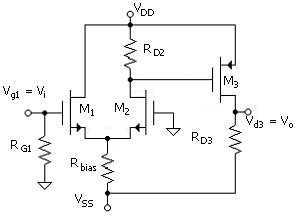
The input can be set equal to zero volts, as it is the gate of a differential amplifier stage in a dual-power-supply configuration. The output can be set equal to zero volts by selecting the drop across the bias resistor RD3 to be equal to |VSS|. This flexibility is provided by the PMOS as the output stage; it is approximately a current course with termination at the negative power supply. With VO = 0, the available output signal range is nearly equal to the magnitude of the power-supply voltage; the drain voltage of M3 can swing anywhere from near VDD down to VSS. Note that this would not be possible if the common-source stage transistor were based on an NMOS.
The output from M2 of the differential-amplifier stage is used arbitrarily. Since the common-source stage is an inverting stage, the gates of M1 and M2 are the inverting (-) and noninverting (+) inputs, respectively. A dc stabilization resistor would be connected between the output (drain of M3) and the input at the gate of M1. This type of feedback would, of course, represent an additional load on the output stage.
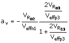
In the example of Fig. 13.1, a differential stage and a common-source stage are connected in a cascade configuration; the input of the common-source stage is the output of the differential stage. The overall voltage gain is defined as av = vo/vi = vd3/vg1. But this is also
Equation 13.1
![]()
Therefore, the gain can be calculated by using the separate expressions considered previously for the differential amplifier stage [( )] and the common-source stage [( This leads to
Equation 13.2
![]()
or using, from ( ), gm = 2ID/Veff,
Equation 13.3
![]()
Throughout this unit, the assumption is made that gm1 = gm2 and veffn1 = Veffn2.
The gain expression neglects the transistor output resistance in the differential amplifier gain for simplicity without a great loss of accuracy, due to the relatively small value of RD2. It also neglects the effect on the gain of the differential stage of Rbias. [Rbias and the output resistance are included in gain result ( ), for comparison.] For a calculation of a numerical value of a representative gain, assume that Veffn1 = Veffp3 = 0.3 V, Vtno = Vtpo = 1.0 V (giving VRD2 = 1.3 V), VRD3 = 5 V (for Vss = -5 V) and lp = 0.05 V-1. The voltage-gain magnitude is |av| = 4.33 · 26.7 = 116. We compare this below with an amplifer that has better bias stability but which loses gain in a trade-off.
The amplifier of Fig. 13.1 is not a good design in terms of bias stability. Bias current ID3 (of M3) in the circuit of Fig. 13.1 is very sensitive to the voltage across RD2, which, in a relative sense, is only marginally predictable, given the normal variation in device parameters and circuit components. Also, as in the bias-stability discussion of Unit 5.5 on the design of the NMOS common-source amplifier, for a constant VGS3, bias current ID3 is sensistive to changes in transitor parameters. (Note that the differential-amplifier-stage bias current is relatvely stable, as it is a current-source bias current.)
As noted, it was shown in Unit 5.5 that a degree of bias stability is provided with a source resistor as in the circuit of Fig. 13.2 (in this case, RS3). This is an additional example of providing some stabilization with the addition of ac and dc negative feedback in a circuit. The addition of the resistor results in an increase in the gain of the differential amplifier stage but a decrease in the gain of the common-source stage. The net result is a reduction of gain as a trade-off between the gain and bias stability.
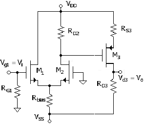
The gain expression for the circuit with RS3 is
Equation 13.4
![]()
where ( ) is now used for the gain of the common-source stage. It is useful again to express the result in terms of Veffn and Veffp and the voltages across resistors to make a quantitative assessment of the gain. Using gm = 2ID/Veff [(4.5)], the gain expression is
Equation 13.5
For example, we set VRS3 = 1 V, with a new VRD2 = 2.3 V. The gain magnitude is now |av| = 7.67 · 4.35 = 33.3, compared with 116 for the circuit of Fig. 13.1. Note that the contribution from the differential stage increases from 4.3 to 7.7.
The output-resistance effect on the gain of the common-source stage is neglected [as in ( ]. This is justified as the output resistance at the drain of M3 is increased significantly with RS3. [Precision gain equation ( ) gives 4.21 compared with 4.35 using ( )]. This is discussed further below in conjunction with the common-source amplifier with source resistor from the viewpoint of a feedback circuit.
If resistor VRS3 is sufficiently large, gm3RS3 >> 1. In this limit the gain is
Equation 13.6
![]()
The magnitude of gain given by ( ) is about 38, a fair approximation to the value of 33 from ( ). It is apparent from the form of ( ) that a significant degree of gain stabilization has been achieved, as the gain depends primarily only on the bias currents ID1 = ID2, which is quite stable in the differential amplifier circuit.
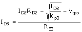
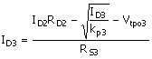
The benefit to ID3 bias stability associated with transistor parameter variation can be assessed by a consideration of ( ) applied to this case, which is
For a quantitative example, suppose that ID3 = 100 mA. To be consistent with the numbers used in Unit 13.2, kp3 = 1110 mA/V2 with Veffp3 = 0.3 V.
Assume that VRD2 = ID2RD2 is constant. Now make kp3 5% larger and Vtpo3 50 mV smaller. For the VRD2 = 2.3 V, we have a new ID3 = 105 mA for VD3 = 0.25 V, which is an acceptable bias value. For the circuit of Fig. 13.1, and the same parameter changes, the new bias current is ID3 = 143 mA for VD3 = 2.15 V, significantly away from the design zero volts.
The actual differential-stage bias current will vary from the basic design due to the variation in circuit components, transistor parameters, and power-supply voltage. Suppose that in lieu of the value of VRD2 = 2.3 V as in the example above, VRD2 is 5% higher or 2.42 V. Assume that the transistor parameters of the common-source stage are at the original design values.
An estimate of the new output voltage (different from 0V) can be made using the linear relation between the input and output of the common-source stage, that is, the common-source contribution of ( ). The "signal" is the change of voltage across RD2, which is -0.12 V. (The gate voltage vG3 decreases.) The common-source gain from ( ) for the original parameters associated with M3 is -4.35. The output bias voltage is now (-4.35)(-0.12V) = 0.5 V (instead of 0 V). Therefore, the circuit is reasonably bias stable.
The gain of the unstabilized circuit of Fig. 13.1 is -27, which leads to an output voltage, for the same change of voltage across RD2, of 3.2 V, using the linear approximation. Note that the linear approximation is marginally valid only for such a large value of the common-source input "signal" voltage, as in this case of no source resistor. (A dc calculation gives a bias output voltage of 4.8 V.)
The circuit of Fig. 13.2 with the source resistor is technically a feedback circuit. It falls into the category of series - series feedback, or the feedback network samples the output current and feeds back a voltage in series (and the same polarity, negative feedback) with the input to the common-source stage, that is, Vgs3. The series - series feedback amplifier is referred to as a transconductance amplifier. The noninverting and inverting opamp configurations are series - shunt (voltage amplifier) and shunt - shunt (transresistance amplifier), respectively. An additional alternative is shunt - series (current amplifier). An example of this type of feedback amplifier is discussed in Unit 13.5
In Unit 9.9, an expression for the output resistance of the current source (drain current) with source degeneration was obtained [( This is
![]()
The perspective of the common-source amplifier in a series - series feedback mode is shown in Fig. 13.3. The circuit configuration is for determining the output resistance. A voltage Vo is applied at the output terminals with the input grounded. In this series - series circuit, a feedback voltage, Vf, which is proportional to the current Io, is induced as indicated in the circuit diagram. With the input grounded, voltage Vf is applied to the input terminals of the transistor. The loop equation at the output is then
Equation 13.7
![]()
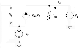
By comparison of the feedback circuit of Fig. 13.3 with the circuit of Fig. 13.2, Vf = IoRS3. Thus,
Equation 13.8
![]()
This produces ( ) from Ro = Vo/Io and with rds = 1/gds. Intuitively, the feedback is such as to cause a much larger current through rds than Io, and therefore a much larger Vo is required for a given Io.
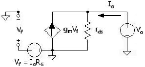
Dropping the RS as in the right-hand side of ( ) renders the result equivalent to the ideal series - series feedback amplifier, as shown in Fig. 13.4. In the ideal series - series amplifier, the sense function has zero resistance; that is, the output voltage is directly across rds. With gm/gds >> 1, the ideal circuit provides a very good approximation to the actual circuit. For example, with Veffn = 0.5 V and ln = 1/50 V, the ratio is 100.
For both feedback amplifier types with series as the second term (series - series and shunt - series), the output resistance is increased by a factor (1 + T), where T is the loop gain, as in the discussion of the opamp feedback amplifiers in Unit 11. The loop gain for the common-source circuit of Fig. 13.2 is, by definition, T = Vf/Vgs3. By inspection of ( ) we conclude that T = gm3RS3. In terms of T, the output resistance is then
Equation 13.9
![]()
The cascading of two common-source amplifier stages will now be explored. This will expand the discussion on feedback amplifiers to include the shunt - series (current) amplifier. As shown in Fig. 13.5, the current Io is sensed, with the feedback network consisting of RS2 and Rf, and a fraction of Io is summed at the gate input node along with the input source current. Gate resistor RG1 provides for an addition bias design variable but otherwise is simply combined with the source resistance, Rs, in the amplifier performance analysis or design.
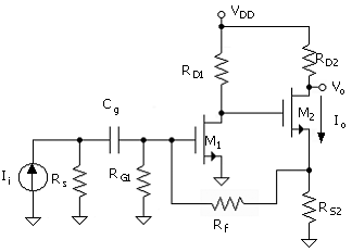
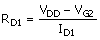
For the design, assume that a choice has been made for ID1 and ID2 and VG2 = VD1. The latter must be such that VG2 > VGS1 + VGS2. Then, for RD1, use
Equation 13.10
As will be indicated below, the ideal current gain is
Equation 13.11
![]()
Use this, based on the feedback-amplifier design current gain goal, to obtain a relation between Rf and RS2. This gives
Equation 13.12
![]()
Now determine the value of RS2 which statisfies the design value of ID2. This is obtaned from
Equation 13.13
![]()
where has been used for Rf and where VS2 = VG1 - VGS2 and
Equation 13.14
![]()
and
Equation 13.15
![]()
Finally, select RG1 to satisfy the VGS1 requirement from
Equation 13.16
![]()
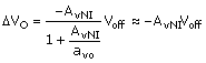
The feedback network provides significant bias stabilization and the effect can be assessed by the same formulation as for the opamp. In Unit 11.4, it was shown that the output voltage for a given offset voltage is [(
As applied to
our shunt - series circuit (by equivalency), AVNI = 1 + Rf/RG1,
and avo is the voltage-gain magnitude (minus terminal equivalent)
from the gate, Vg1, to the source Vs2, that is, the gain
of the case of a common-source stage (M1) and a source-follower
stage (M2). Also, for this case, DVo ![]() DVS2. Note that for this case, DVo is a bias-voltage change, whereas for the opamp, it is the
output voltage (different from zero volts).
DVS2. Note that for this case, DVo is a bias-voltage change, whereas for the opamp, it is the
output voltage (different from zero volts).
Suppose that
the dc (bias) is at a set state. Then the bias is altered such as by a change
of a transitor parameter (either by temperature change or substituting one
transistor for a new one). For example, a change in Vtno of M1
is equivalent to installing an offset voltage, and [( )] can be applied directly to this
case. Make RG1 = Rf for AVNI = 2. Also assume
a typical avo = 40 (common-source stage). For a change of dVtno ![]() -Voff = -0.1 V, DVO
-Voff = -0.1 V, DVO ![]() 2 · 0.1 V = 0.2 V. Note that based
on avo = 40, with no feedback stabilzation, the change in output
would be approximately avodVtno
= 4 V.
2 · 0.1 V = 0.2 V. Note that based
on avo = 40, with no feedback stabilzation, the change in output
would be approximately avodVtno
= 4 V.
We first compute the open-loop transconductance and then the open-loop current gain. This is done, for a good approximation, by disconnecting the right side of Rf from the souce of M2 and connecting it to ground. (This disables the shunt - series feedback and otherwise alters the circuit only slightly.) The result is
Equation 13.17
![]()
where Ri = Rs||RG1||Rf. (This assumes that Rf >> RS2 which is consistent with AiI >> 1.) Transconductance Gm is for the complete cascade circuit (open loop), that is,
Equation 13.18
![]()
Note that the series - series feedback effect is retained in the open-loop computation and that RS2 has been used as an approximation for RS2||Rf. This once again assumes that Rf >> RS2. The loop gain is
Equation 13.19
![]()
Following the discussion in Unit 11, which led to ( ), the current gain with feedback is then
Equation 13.20
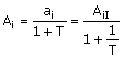
where (ideal current gain of the feedback amplifier)
Equation 13.21
![]()
As a design example, suppose the design goal is AiI = 10. Assume that the transistors have Vtno = 1 V, kn1 = 1000 mA/V2, and kn2 = 2000 mA/V2. We select ID1 = 100 mA, ID2 = 200 mA, VDD = 10 V, and VG2 = 3.5 V. From ( ) and ( ) we obtain RS2 = 11.4 kW and Rf = 103 kW. Based on ( ), the value of RG1 is RG1 = 156 kW. To satisfy the drain voltage requirements, RD1 = 65 kW and RD2 = 25 kW. The latter is based on VD2 = VDD/2. Also, we assume that Rs = 100 kW
The open-loop
transconductance is Gm = 3372 mA/V and Ri
= 38 kW for ai = 129. Loop gain T = 12.9
such that Ai = 9.28. We note that since Ai ![]() AiI = 10, the current
gain is very predictable, despite bias and parameter variations.
AiI = 10, the current
gain is very predictable, despite bias and parameter variations.
|
|
Gain of cascade of differential stage and common-source stage, including output resistance of M3. |
|
|
Gain of cascade circuit for case of common-source stage with source resistor. |
|
|
Approximate form for gain which assumes that gm3RS3 >> 1. |
|
|
Bias equation for transistor M3. |
|
|
Shunt - series amplifier dc design equations. |
|
|
Shunt - series amplifier dc stability relation. |
|
|
Shunt - series amplifier open-loop current gain relations. |
|
|
Feedback amplifier current-gain relations. |
|