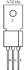
PB.1 SPICE Parameters and Transistor Diagram
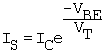
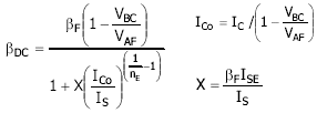
PB.2 SPICE Equations
PB.3 Diode-Connected Transistor Measurements
PB.4 Measurement of bDC versus the Collector Current
PB.5 BJT Output Characteristic Measurement
PB.6 Simulation of the Output Characteristic Measurement
Exercises and Analysis ExerciseB.mcd-ProjectB1.mcd-ProjectB2.mcd-ProjectB3.mcd
|
SPICE PARAMETERS |
|
||
|
SPICE Name |
Math Symbol |
Description 555h718f |
|
|
IS |
IS |
Saturation current. |
|
|
NF |
nF |
Forward-current emission coefficient. |
|
|
ISE |
ISE |
Base - emitter leakage saturation current. |
|
|
BF |
bF |
Ideal maximum forward current gain. |
|
|
NE |
nE |
Base - emitter leakage emission coefficient. |
|
|
VAF |
VA |
Forward Early voltage. |
|
|
BR |
bR |
Reverse current gain. |
|
|
SPICE Equation |
Description 555h718f |
|
|
|
B.6 |
Dc ratio of collector current and total base current. |
|
|
From B.7 |
Collector current to base - emitter voltage relation for VBC = 0 V. |
|
|
B.25 |
Form of (B.7) to calculate IS. |
|
|
B.7 |
Active-mode collector current to base - emitter voltage relation. |
|
|
B.10 |
Ideal base current. |
|
|
B.12 |
Total base current in the active mode. |
|
|
B.23 |
General equation for collector current versus terminal voltages of the common emitter. |
|
|
B.26 |
General equation for collector current with base leakage current and an artificial bR |
|
|
B.38 |
Dc beta versus collector current. |
|
Components
Exercise care when forcing the transistor into the circuit board. LabVIEW Computations
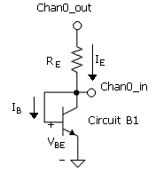
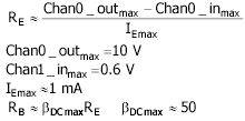
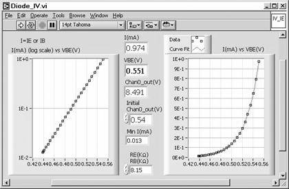
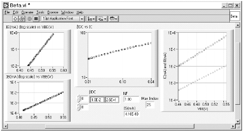
Slope is from curve fit of ln(IC) vs. VBE Procedure Diode_IV.vi is used to obtain the current - voltage characteristic for Circuits, B1 and B2. The results will be installed into two Control Graphs of Beta.vi (below). Running Beta.vi then produces values for IC, bDC versus IC, and parameters nF and IS. Connect Circuit B1. In the Front Panel of Diode_IV.vi, set the value of RE. Run Diode_IV.vi and re-run while resetting Initial Chan 0_out for Min IE of about 0.01 mA. The VI will halt for IE=1 mA or Chan0_out=10 V. Obtain a log of the results. Default the Front Panel to save Initial Chan0_out. It is used in the next circuit. Connect Circuit B2. Set the value of RB. Run the VI. It will halt for Chan0_out at about 10 V. Obtain a log of the results.
Open Beta.vi. Copy the IE and IB data from the graph (log scale) of Diode_IV.vi and paste the data into the Control Graphs IE (log scale) versus VBE and IB versus VBE, respectively. These data are saved in the log of the Front Panel of Diode_IV.vi. (Reminder: For data copy and paste, Right Click on graph face and Data Operations/Copy or Paste.) Default and save Beta.vi. Run the computation VI, Beta.vi. Beta.vi will compute and plot bDC versus IC and indicate parameters nF and IS. Note that the plot uses the values of VBE from the data of IE. An interpolation of the VBE values of IB then is made to find the corresponding IB values.
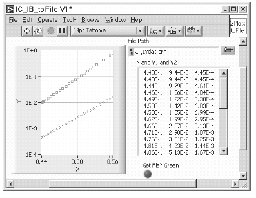
Beta.vi finds the highest VBE on the low end (for IE or IB) and the smallest VBE on the high end, such that the two plots coincide over the full range of VBE in the combined-plot graph. Note the VBE scale in the right graph of Beta.vi. The computation of NF uses thermal voltage, VT, computed for T = 27°C. At the low currents of the measurements, the device heating is probably negligible and the transistor temperature is probably about 27°C. Obtain a data file of measured IB and IC for use in a Project B Mathcad file, ProjectB1.mcd. Open IC_IBtoFile.vi (below) from the ProjectB.llb. Copy and paste the plots in the graph on the right side of Beta.vi into the Control Graph of IC_IBtoFile.vi. Write your file path and file name. The file must appear in the folder with the ProjectB1.mcd.
For simulation only, copy and paste the data stored in the log of the Front Panel of Diode_IV.vi. Follow the procedure for Beta.vi above. |
PB.4 DC versus the Collector Current Measurements
bDC versus the Collector Current" href="?x=1&mode=section&sortKey=title&sortOrder=asc&view=&xmlid=0-13-047065-1/ch31lev1sec4&open=true&g=&catid=&s=1&b=1&f=1&t=1&c=1&u=1&r=&o=1&srchText=" class="v2">Measurement
|
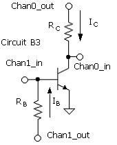
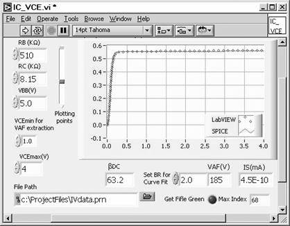
Components Same circuit as in PB.4 LabVIEW Computations SPICE IC versus VCE. This is performed with subVI SPICE.vi. Straight-line curve fit from active-region data:
ICo VAF = Slope/ICo Procedure Open subVI, IC_VCEsub.vi. This VI
will send out a value of VBB and sweeps VCC to sweep VCE. The maximum VCE is
set for 4 V. Set the value of the resistors. Run
and re-run while setting VBB for an
active-region collector current of about 0.5 mA. Note that at this collector
current, a maximum VCE of 4 V should be attainable as the circuit was
designed (PB.3 PB.4) for ICmax
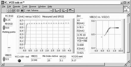
Now open VI, IC_VCE.vi. Set the value of the resistors. Set VBB from the subVI, IC_VCEsub.vi. Set VCEmax at 1 V. Run the VI and adjust BR for a best fit. Then re-run the VI with VCEmax set at 4 V to obtain a good value for VAF. VAF is computed from data points in the range 1 < VCE <VCEmax. Default and save the Front Panel. Double check to be sure that the subVI is defaulted and saved. The data are used in the output characteristic measurement simulation.
|
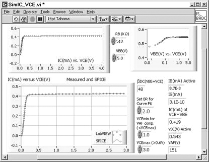
|
Procedure SimIC_VCE.vi simulates the output characteristic measurement and associated curve fitting. Data are supplied from an actual measurement from any sample IC_VCEsub.vi. The data include IC versus VCE and VBE versus VCE. Copy and paste the two data sets from the sample (saved Front Panel or log data) IC_VCEsub.vi. Set up all values in the Digital Controls. The information will be used to compute and display the output characteristic, measured and SPICE, and various parameters and dc variables in the Digital Indicators. Parameters bDC and IS are computed for VCE = VBE, according to the definitions. VAF is computed from a selected range of bDC from the active region. (Continued below.)
Run the VI and re-run while adjusting BR for the best fit. Use a small VCEmax for this. Verify that VCEmin < VCEmax for this simulation. Note that for the best fit, the SPICE curve goes from slightly greater to slightly less than the measured data with increasing VCE in the saturation region. Re-run for computing VAF in various ranges (e.g., 1 V to 3 V, 2 V to 4 V, etc). Note that VAF varies, and depends on the voltage range, unlike the ideal SPICE basic model. Of primary interest is the evaluation range of 1 V to 3 V, as this brackets the bias voltage of 2 V of the amplifier project, Project C1 Default this case. Note also that the curves will fit in the active region for any combination of VBB and RB. However, the bDC value will only be correct for the actual circuit values. For clarity on this point and others, the computations will be repeated in the Mathcad project file. Save the results. |
|