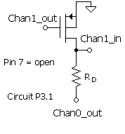
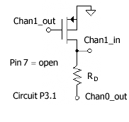
P3.1 SPICE Parameters and Pin Diagram
P3.2 SPICE Equations
P3.3 PMOS Transistor
P3.4 Low-Voltage Linear Region of the Output Characteristic
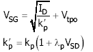
P3.5 PMOS Parameters from the Transfer Characteristic
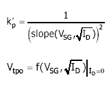
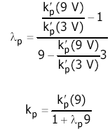
P3.6 PMOS Lambda from the Transfer Characteristic
P3.7 PMOS Output Characteristic
P3.8 PMOS Lambda
Exercises and Analysis Exercise03.mcd - Project03.mcd
|
SPICE PARAMETERS |
||
|
SPICE Name |
Math Symbol |
Description |
|
VTO |
Vtno, Vtpo |
Zero VSB threshold voltage. |
|
KP |
|
Transconductance parameter. |
|
GAMMA |
gn gp |
Threshold voltage parameter. |
|
LAMBDA |
ln lp |
Active-region slope parameter. |
|
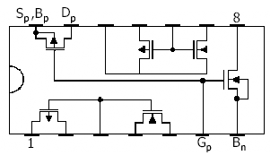
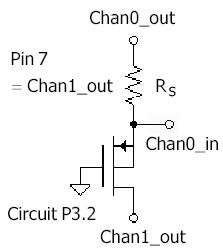
CD4007 Pin Diagram
|
||
|
SPICE Equation (PMOS) |
NMOS Eq. |
Description |
|
|
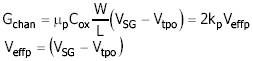
Output characteristic low-voltage conductance. |
|
|
|
Output characteristic for full linear range (0<VSD<Veffp). |
|
|
|
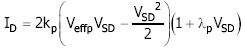
Active region transfer characteristic and output characteristic (VSD>Veffp). |
|
|
|
Active region relation solved for VSG. |
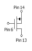
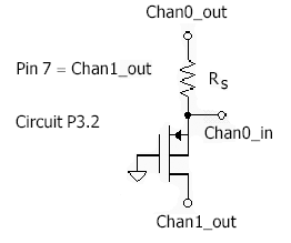
Use pins 6 (gate), 14 (source), and 13 (drain). Connect the NMOS body (pin 7) to the most negative node, Chan1_out, for PMOSparam.vi. Leave pin 7 disconnected when running PMOSoutput.vi. Note that the source and body for this transistor are internally connected. Note that Chan0_in is used for positive voltages only. Thus, it is always set automatically for the unipolar mode, which slightly improves the resolution. Chan1_in must measure positive and negative voltages.
![]()
|
Components
LabVIEW Computations
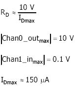
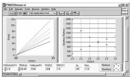
Procedure Run PMOSlinear.vi and adjust VSGstart(V) such that Veffpstart(V) > 0.5 V. The maximum ID is set for 0.1 V. Run the VI to obtain parameters as indicated in the Front Panel. Default and save the Front Panel to save information for the Mathcad analysis. |
|
Components
LabVIEW Computations
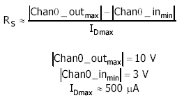
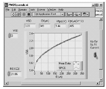
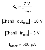
Procedure Run PMOSparsub.vi with VSD = 3 V and VSD = 9 V. VDD (Chan0_out) starts at 2 V such that the minimum current is IDmin = (2 V - VSGmin)/RS. ID stops automatically at ID = 500 mA or Chan0_out = 10 V. Verify that the VI functions properly. PMOSparsub.vi will run as a subVI of the next VI. |
|
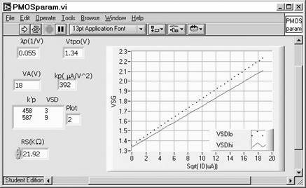
Components
LabVIEW Computations
Procedure Run PMOSparam.vi to run subVI PMOSparsub.vi at VSD = 3 V and VSD = 9 V to resolve Lambda and final values of kp and Vtpo. Default and save the Front Panel to save the parameter values for the Mathcad results analysis file. |
|
Components
LabVIEW Computations Linear Region
Active Region
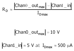
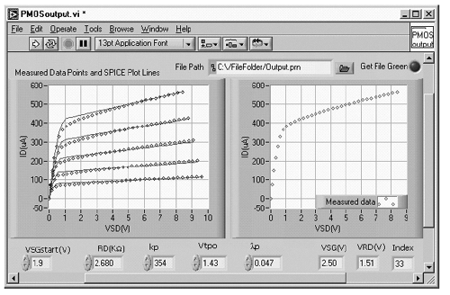
Procedure Install PMOS parameters from P3.6 into the Front Panel of PMOSoutput.vi. A given VSD sweep will halt at
Chan0_out = 10 V. Set VSGstart(V) as necessary to
obtain ID With the data defaulted and saved in the graph of the VI, a data file can be obtained at a later time. From the Diagram of PMOSoutput.vi, click on XYtoDataFile.vi, copy the data from PMOSoutput.vi, and paste it into the Control Graph of XYtoDataFile.vi. Name the path and data file and run the VI. XYtoDataFile.vi is located in the User.lib in the LabVIEW folder. Therefore, it can also be opened from the Diagram of a VI under Functions>>User Libraries>>Dat_File. |
|
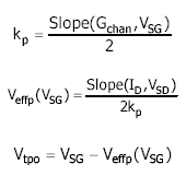
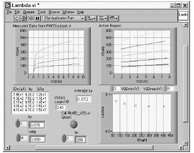
LabVIEW Computations Straight-line curve fit from active region data: ID = Slope · VSD + IDo lp = Slope/IDo kp = IDo/Veffp2 Procedure Lambda.vi is configured for Enable Data Base Access to read the data from PMOSoutput.vi. Lambda.vi can read all of the Front Panel information in PMOSoutput.vi when a log of the Front Panel has been obtained. From the Diagram of Lambda.vi, open PMOSoutput.vi. Obtain a data log of the Front Panel of the PMOSoutput.vi (under Operate Menu). Run Lambda.vi to read the graph of measured data (from PMOSoutput.vi) and to plot the measured data from the active region. The VI obtains Kp and lp from these data, for each of the voltage sweeps. Note that Lambda varies. Compare the average Lambda value with that from PMOSparam.vi. Click on Call PlotID_VSD.vi Green to bring up a plot of the active-region equation plot for -1/lp < VSD < VSDmax, compared with the measured data. Lambda.vi will be used in the Mathcad analysis file.
|
|