The amplifier in this part is the same, in principle, as the basic common-source amplifiers of Figs. 2.4 and . However, now the actual resistor RD is replaced with a current-source load as shown in the circuit of Fig. 10.1. As noted in Unit 9, a benefit of replacing bias resistors with current sources is a reduced requirement for resistors in the circuit; the reference voltage associated with M3 can be used elsewhere in a typical circuit. Additionally, as will be shown, the gain of the common-source stage is substantially imp 313e418d roved over that with actual bias resistor RD. The specific circuit of Fig. 10.1 is that for the project amplifier. The bias and gain of the amplifier are evaluated in the following.
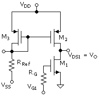
The bias circuit is critical in terms of getting the dc output voltage at a value near the project design value of VO = VDD/2 (for maximum output magnitude and linearity). The relation, from the dc circuit analysis, for obtaining this condition is based on ID1 = ID2. This is, in terms of the transistor characteristic equations, (
Equation 10.1
![]()
Note that the source-gate voltage of M2 is referenced to M3. A certain combination of VGS1 and VSS will satisfy Vo = VDD/2. In the project on the amplifier, a LabVIEW VI sends out a VG1 = VGS1 to set up a given ID1 = ID2 and then adjusts VSS to obtain the desired bias output voltage.
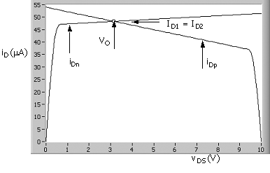
Figure 10.2 shows a SPICE plot of the current for the PMOS and NMOS transistors as a function of VDS1. The source - drain voltage for the PMOS is VSD2 = VDD - VDS1. Both transistors have a specific gate - source voltage. The solution for the output voltage for this case is about 3 V. A slight decrease in VGS1 or a slight increase in VSG2 is required to bring VDS1 to 5 V, the design result in this example. The increase in VSG2 would be implemented by making VSS more negative to increase the reference current. The steeper slope in the active region of the PMOS device is consistent with lp > ln, as in the project amplifier.
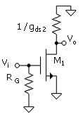
The expression for the gain of the basic common-source amplifier, ( ), which includes the output resistance of the driver transistor, is
![]()
In the signal circuit, as shown in Fig. 10.3, RD is replaced by 1/gds2. The new equation for this circuit is
Equation 10.2
![]()
or with gm
= 2ID/Veff, ( ), and gds ![]() ID l
ID l
Equation 10.3
![]()
The result shows that the gain increases for decreasing Veffn1. This is limited by the fact that the MOSFET ceases to behave in the normal manner at some lower limit on Veffn.
Using ![]() an alternative form is obtained,
which reveals the ID1 dependence of the gain. This
is
an alternative form is obtained,
which reveals the ID1 dependence of the gain. This
is
Equation 10.4
![]()
Increasing gain is achieved with decreasing the level of bias current. The lower limit is, as noted above, associated with a lower limit on Veffn. Also, there is an approximate inverse trade-off between frequency response limitations, on the high end of the spectrum, and gain.
The gain, though, for the amplifier with current source load, will generally be several times as large as that with the resistive load. An amplifier with even higher gain can be obtained by replacing the current source load with one with source degeneration as discussed in Unit 9.2, and as discussed extensively for the case of the BJT in Unit C
|
|
Output drain-current balance equation. |
|
|
Voltage-gain equation. |
|
|
Voltage-gain equation in terms of l's and Veffn1. |
|
|
Voltage-gain equation in terms of l's and ID. |
|
Project Mathcad Files |
Exercise10.mcd - Project10.mcd |
|
Laboratory Project 10 |
Current Mirror and Common-Source Amplifier with Current-Source Load |
|
P10.2 |
Evaluation of the Current-Source Circuit |
|
P10.3 |
Evaluation of the Mirror-Current Circuit |
|
P10.4 |
Evaluation of the Bias Setup |
|
P10.5 |
Measurement of the Amplifier Gain versus Drain Current |
|
