As noted in Unit 1, due to the external capacitors that are attached to the circuit for configuring the signal circuit, the gain of the amplifiers will tend to fall off at the low-f 616t194g requency end of the frequency spectrum. The design basis for choosing the capacitors for a given application is considered in the following. The gain-frequency dependence due to the input coupling capacitor, the source-resistor bypass capacitor, and the load coupling capacitor is discussed. A discussion of response roll-off on the high end of the spectrum is deferred to Unit 11
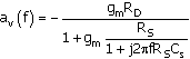
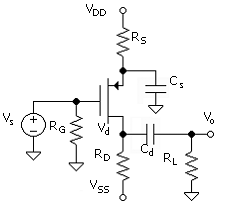
A version of the circuits of Fig. 5.2, as given in Fig. 6.1, is generalized to include a resistance, Rs, as part of the input signal source. The input signal at the gate (and thus the output) will fall off for decreasing frequencies as the magnitude of reactance of the capacitor increases. The value of the capacitor is selected such that the reactance will be small compared to the value of the sum of the resistors, at the lowest operating frequency.
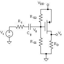
In this amplifier, all the gain-frequency dependence is between Vg and Vs. The relation between the gate signal, Vg, and source signal, Vs, based on a voltage-divider relation is
Equation 6.1
with
Equation 6.2
![]()
where RG = RG1 || RG2.
With Rs included, the f3dB expression applies to an actual amplifier. In Project 6, the signal-source voltage is applied directly to the gate. We select a combination of RG and Cg to obtain a suitably low f3dB. This must be more than a factor of 10 lower than the gain measurement frequency assure that the capacitor is not influencing the measurements.
In Projects 5 and 7, no capacitor is used at the input as the signal is superimposed on the dc gate voltage. This is to facilitate the need for both DAQ output channels to provide the bias. However, Project 6, one channel provides the bias, as in Figs. 5.1(a) and , and the other channel is used for the signal with connection to the input through a coupling capacitor.
The PMOS common-source amplifier circuit with the bypass capacitor is shown in Fig. 6.2. At some low frequency, the effect of the capacitor is absent, and the gain is computed from ( ), which is
![]()
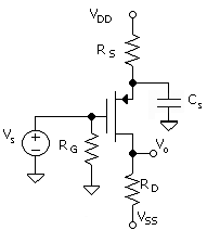
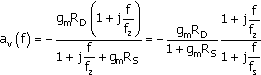
Over a range of frequencies, the gain evolves from ( ) to ( ), av = -gmRD (neglecting the output resistance of the PMOS). The frequency-dependent transition region is determined by replacing RS in ( ) with the impedance of RS in parallel with the reactance of Cs. This is
Equation 6.3
or
Equation 6.4
with
Equation 6.5
![]()
and
Equation 6.6
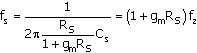
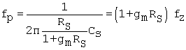
Note that the "RC" factor has an "R," which is RS in parallel with 1/gm, the latter being the output resistance looking into the source of the transistor. The two frequencies fs and fz are technically the pole and zero of the response function.
We note that
gmRS = 2IDRS/Veffp.
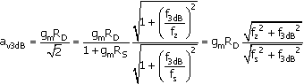
Since Veffp could be as low as Veffp ![]() 0.2 V, then gmRS >> 1 in some cases. The corner frequency, f3dB, occurs at
0.2 V, then gmRS >> 1 in some cases. The corner frequency, f3dB, occurs at
Equation 6.7
which gives
Equation 6.8
![]()
such that
Equation 6.9
where the far-right-hand term applies for gmRS >> 1. This is typically only marginally satisfied in MOSFET circuits.
The derivation carried out here was initiated from ( ), which neglects the output resistance of the transistor. In the case of the MOSFET devices of our projects, the simplification is valid for the NMOS transistor but marginal for the PMOS transistor. This is because lp >> ln. The result ( ) still serves to estimate the required value for Cs, even for the case of the PMOS. Nevertheless, a more detailed derivation is carried out in the next unit. This permits comparisons, in a project, of SPICE and Mathcad solutions with amplifier gains and frequency response.
In Unit 8, the gain of a common-source stage with source resistor, which includes the effect of the output resistance, is shown to be [(
![]()
This is designated here as avolo to emphasize that it is the constant low-frequency asymptotic gain. If the source-branch impedance is substituted for RS, this becomes
Equation 6.10
where fz is ( ). This can be rearranged in the form of ( ), which is
Equation 6.11
where the new pole frequency is
Equation 6.12
![]()
and avolo is (
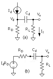
The complete
practical amplifier includes a load, RL, at the output. This
requires an additional coupling capacitor. The amplifier with an attached load
is shown in Fig.
6.3.
We will assume that the effect of the output resistance, rds, can be
neglected. The transistor appears as a current source of magnitude
Equation 6.13
![]()
The expression with the high-frequency asymptotic value and frequency dependence is
Equation 6.14
![]()
which is
Equation 6.15
![]()
where
Equation 6.16
![]()
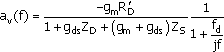
Current source Id is not dependent on frequency (at the low end of the spectrum) when no other capacitors are considered. However, in general, with both Cd and Cs attached, the combined response is
Equation 6.17
where fd
is ( ), fz is ( ), fs is ( ), and ![]() is RD in parallel with RL.
With Cd = Cs, usually fd
<< fs such that ( ) is the approximate f3dB
for the circuit with both capacitors connected.
is RD in parallel with RL.
With Cd = Cs, usually fd
<< fs such that ( ) is the approximate f3dB
for the circuit with both capacitors connected.
Combining the frequency-dependent terms to obtain ( ) assumes that current source Id is independent of components Cd, RD, and RL. This is a correct assumption as long as the output resistance of the transistor is neglected. When better precision is required, the derivation starts with the general form of the circuit transconductance, as deducible from ( ), and replaces both RD and RS with the impedance in those respective branches, ZD and ZS. This gives
Equation 6.18
![]()
The gain follows from multiplying the transconductance by the load at the drain, ZD, and multiplying by the voltage divider, Vo/Vd = RL/(RL + 1/j2pfCd). The result is
Equation 6.19
|
|
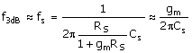
MOSFET coupling capacitor corner-frequency equation. |
|
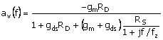
|
Zero and pole equations for bypass capacitor response function. |
|
|
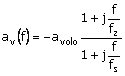
Computation of f3dB frequency with one pole and one zero. |
|
|
Approximate f3dB frequency for capacitor Cs. |
|
|
Pole frequency fs with gds included in the derivation. |
|
|
Load coupling capacitor corner-frequency equation. |
|
Note: Any one of the frequencies, fg, fs (approximate), or fd is the f3dB (corner) frequency if it is the dominant (high) frequency. Otherwise, the corner frequency is some combination. |
|
|
Project Mathcad Files |
Exercise06.mcd - Project06.mcd - Exercise07.mcd, Project07_1.mcd - Project07_2.mcd. |
|
Laboratory Project 6 |
PMOS Common-Source Amplifier Stage with Current-Source Biasing |
|
P6.3 |
PMOS Current-Source Amplifier DC Setup |
|
P6.4 |
Amplifier Gain |
|
P6.5 |
Amplifier Frequency Response |
|
Laboratory Project 7 |
NMOS Common-Source Amplifier Stage with Source-Resistor Bias |
|
P7.2 |
NMOS Common-Source Amplifier DC Evaluation |
|
P7.3 |
Amplifier Gain at Optimum Bias for Linear Output |
|
P7.4 |
Optimum Bias Stability Test |
|
P7.5 |
Amplifier Frequency Response |
|