In this unit, we start with the basic components of amplifiers that have been discussed and progress, stepwise, toward an actual integrated-circuit operational amplifier. The final amplifier consists of two gain stages and a buffer stage. The gain stages are the equivalent of the cascade of a differential stage and a common-source stage of Unit 13, except with improvements consisting of current-source bias in place of bias resistors.
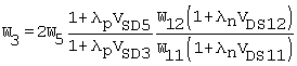
The drain-current bias resistor, Rbias, of the basic differential amplifier stage as introduced in Fig. 8.1 will now be replaced by a current source as shown in the circuit of Fig. 14.1. The bias resistor is replaced by two transistors, M10 and M11, and one resistor, R1. This seems like an unfavorable exchange but it is not. This is because the reference voltage VGS10 formed by the reference circuit of R1 and M10 can be used for additional current sources in the complete circuit, thereby eliminating the need for a number of other bias resistors.
Resistors in an integrated circuit cost much more in chip space than do transistors. Also, the output resistance of a current-source transistor, M11, will be much higher than the resistor equivalent, leading to improved amplifier characteristics, as discussed below.
Following the discussion of transistor current sources in Unit 9, the ratio of the reference current and the current-source current is
Equation 14.1
![]()
The ratio of
the gate widths will thus be selected to satisfy the design of the
differential-stage bias. The current ratio will deviate from the simple ratio
due to the ln terms, but this is not critical, as the design
will not call for an exact value for ID1 ![]() ID2.
ID2.
As discussed in Unit 8, the common-mode gain is the gain for the same signal being applied to both inputs. In Unit 8.6 the common-mode voltage gain expression, ( ), was obtained for the bias resistor, Rbias. This is
![]()
To apply the common-mode gain equation to the circuit of Fig. 14.1, resistor Rbias is replaced by rds11. The result for the common-mode gain is
Equation 14.2
![]()
The
approximate form is consistent with neglecting the change of the gate - source
voltage compared to the change of voltage at the drain of the current-source
transistor, M11. Intuitively, ( ) indicates that for rds11
![]()
![]() , transistor M11, is a pure current source, and iD1
= iD2 = ID1 = ID2 regardless of the magnitude
of common voltage applied to both gates. In this case, signals Id1 =
Id2 = 0 for any (realistic) common-mode input signal.
, transistor M11, is a pure current source, and iD1
= iD2 = ID1 = ID2 regardless of the magnitude
of common voltage applied to both gates. In this case, signals Id1 =
Id2 = 0 for any (realistic) common-mode input signal.
Common-mode inputs can be a form of noise, and therefore the ideal opamp would reject these signals entirely. An important consideration is the extent of rejection based on the common-mode gain relative to the differential amplifier gain. This is quantitatively assessed with the common-mode rejection ratio, which is the ratio of the differential amplifier gain with differential output divided by the common-mode gain, ( ). The gain for this case was obtained in Unit 8.5 as ( ), which is avd12 = -gmRD.
Using ( ) and ( ), the common-mode rejection ratio is
Equation 14.3
![]()
With gm1
= 2ID1/Veffn1 [( )], and for the output resistance of
M11, rds11 ![]() ln2ID1 [( )], the common-mode rejection ratio
is
ln2ID1 [( )], the common-mode rejection ratio
is
Equation 14.4
![]()
By comparison, for resistor bias, the equivalent result is
Equation 14.5

where Rbias is the bias resistor of, for example, the circuits of Figs. 13.1 and
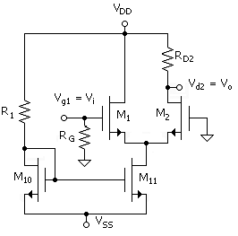
We now add to the differential stage the common-source stage to obtain a two-stage amplifier as in Unit 13 Fig. 14.2). Transistor M12, which replaces bias resistor RD3, provides a current-source load as in the circuit of Fig. 10.1. Note that current ID12 mirrors ID10 and no additional resistors are required with the addition of the common-source stage. That is, M11 and M12 both use the reference voltage provided by the diode-connected M10.
The bias design for the common-source stage consists of picking W12 to obtain a specified ID12 relative to ID10 and making ID3 = ID12. Parameter W12 is determined from
Equation 14.6
![]()
The approximation is sufficient, as the current magnitude, again, is not critical.
The circuit is adjusted to make ID3 = ID12 by equating the relations for the two currents. This is
Equation 14.7
![]()
A much simpler equation replaces this rather complicated one when RD2 is finally replaced by a transistor as well. Veff12 is known from Veff12 = Veff10. Thus, the current balance can be obtained by a selection of the various remaining parameters.
The load on the common-source stage is now rds12 = 1/gds12. The gain is, including the output resistance of M3.
Equation 14.8
![]()
The overall amplifier gain, av = Vo/Vi, is now
Equation 14.9
![]()
This can be evaluated with
Equation 14.10
![]()
Using the numbers from the previous calculation for the amplifier of Fig. 13.1 with RD3, and adding ln lp, the gain magnitude for the circuit of Fig. 14.2 is 289. This compares with the value of 116 for the cascade amplifier of Fig. 13.1. In the next unit, the differential stage will be modified to include a current source load with a considerable additional improvement in gain.
The load resistor (or bias resistor) of the differential stage will now be replaced with a current-source load. In addition to eliminating the need again for a resistor, it provides for much better dc stability and a significant gain improvement, including the elimination of the factor of ½ associated with the differential stage gain as in ( ) and (
As shown in the new circuit in Fig. 14.3, the resistor RD2 is replaced by transistors M4 and M5. Transistor M5 provides a current-source load for transistor M2. The diode-connected transistor, M4, provides the dc reference voltage for M5. The reference current is ID1 = ID4.
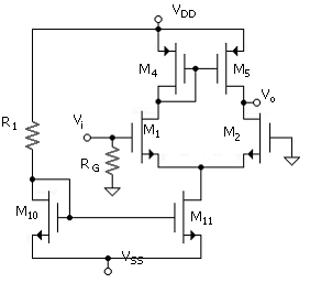
The dc output voltage (of the differential stage) is set automatically at VDD - VSG4 due to the relation VSD4 = VSG4 = VSG5 = VSD5. This is an idealization that assumes that the parameters of transistors M4 and M5 and M1 and M2 are identical and that ID1 = ID2.
Recall that in the differential stage with drain resistor, RD2, the noninverting output signal voltage was induced across RD2 due to the signal current Id2. In the new circuit, the output current is the composite of signal currents Id2 and Id5. That is, signal current Id1 is mirrored at the output as Id5. This is a result of the coupling from M1 through M4 to the gate of M5. The circuit from the gate of M1 to the drain of M5 can be regarded as a cascade of two common-source stages (M1 and M5) with a shunt resistor between them of magnitude 1/gm4 (the signal resistance of the diode-connected transistor).
The gain for this circuit can be explained starting from the transconductance for the two currents Id2 and Id5. Assume for a moment that the output voltage is held constant at the dc bias value. This is equivalent to a signal short circuit at the output. As in the case of the resistor-bias differential amplifier stage, we have
Equation 14.11
![]()
where the effect of the output resistance of M11 is neglected. But also, as in the resistor-load case,
Equation 14.12
![]()
But Id1 = -Id4 and Id4 is mirrored as Id5, which leads to Id5 = -Id1. This assumes that M4 and M5 are identical. Thus,
Equation 14.13
![]()
All signal drain currents are defined as positive into the respective drains.
The output currents summed at the output node, Vo, are (defined positive into the node)
Equation 14.14
![]()
The result is valid for vO = VO or Vo = 0, as stipulated above. One could imagine attaching a dc supply exactly equal to VO at the output node. In this case, the output current could readily flow into the node according to (
For the opposite extreme of having an open circuit at the output, as in Fig. 14.3, the currents Id2 and Id5 are dependent on vD2 = vD5 = vO. The deviation of Io from ( ) is, as usual, taken care of by including the effect of the output resistance at the output node.
The output resistance is somewhat complicated by feedback effects, which are inherent in this circuit. For assessing the circuit output resistance, a signal circuit is shown in Fig. 14.4 with a test voltage, Vo, applied at the output with both inputs grounded. Resulting currents Id2 and Id5 will be considered separately and will be superimposed.
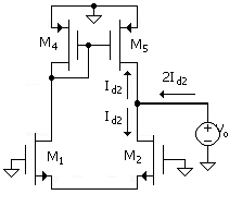
The currents indicated in Fig. 14.4 are for the case of Id2 of M2. Looking back into the drain of M2, the output resistance is affected by emitter degeneration because of the resistance 1/gm1 between the emitter of M2 and ground. That is, the resistance looking back into the emitter of M1 is 1/gm1. Thus, the resistance looking only back into M2 is 2rds2. However, Id2 feeds through and around the loop composed of M2, M1, M4, and M5 such that the total current flowing into the node (exclusive of the separate Id5 contribution) is 2Id2. The test voltage is Vo = Id22rds2, due to current Id2 flowing down into the resistance 2rds2 of the drain of M2. The output resistance associated with the drain of M2, RoM2, is based on a total current of 2Id2 such that it is
Equation 14.15
![]()
The drain resistance 2rds2 combined with a test current of 2Id2 results in an effective drain resistance rds2 despite the emitter degeneration.
Separately, by superposition, for applied Vo, a current Id5 of value Id5 = Vo/rds5 flows into the drain of M5 such that the output resistance associated with M5 is RoM5 = rds5 = 1/gds5. This is based on the fact that the output resistance is that of a common-source stage with grounded source. The two contributions are in parallel such that finally, the output resistance is
Equation 14.16
![]()
Combining this with the effective amplifier transconductance obtained above, ( ), the gain is
Equation 14.17
![]()
or
Equation 14.18
![]()
An external load, RL, appears in parallel with Ro. Hence with an external load, the gain is
Equation 14.19
In the discussion leading to ( ), it was noted that the output current given by ( ) is for a short-circuit condition at the output, and the effect of finite Vd2 = Vd5 is taken care of through the concept of the output resistance of the circuit. A clarification of this statement is provided by the analytical formulation, which includes a load, RL, given by
Equation 14.20
![]()
where vD5 = vD2, as they are the same node. The linear form is
Equation 14.21
![]()
and this
leads to ( ), where, again, av2 = Vd2/Vg1.
A voltage source attached to the output is equivalent to RL ![]() 0, in which case Vd2
0, in which case Vd2 ![]() 0 and vD2
0 and vD2 ![]() VD2 = VO, that is, the bias value. The finite
output current magnitude into the short circuit is consistent with Vd2/RL|vds,
RL
VD2 = VO, that is, the bias value. The finite
output current magnitude into the short circuit is consistent with Vd2/RL|vds,
RL![]() = gm1Vg1.
= gm1Vg1.
As may be deduced from the common-mode gain equation, ( ), in Unit 14.2, the common-mode transconductance for the differential stage with current-source biasing is Gm = gm1/(1 + gm12rDS11). The incremental load at the drain of M1 for the case of the circuit shown in Fig. 14.3, however, is the resistance of the diode-connected transistor M4 of Fig. 14.3, which is 1/gm4. Due to symmetry, this is also the effective load at the drain of M2. The common-mode gain is thus
Equation 14.22
![]()
and the common-mode rejection ratio is, from ( ) (for single-ended output) and (
Equation 14.23
![]()
This is
greater than ( ) by the factor gm4/(gds2
+ gds5) ![]() [Veff4(ln lp
[Veff4(ln lp
The cascade
amplifier that includes all features discussed up to this point is given in Fig.
14.5.
Note that the only (internal) resistor is that of the reference-current
circuit. Bias currents for this circuit can be set up using gate-width
proportions. We note that ID3 ![]() ID5 since M3 and M5 have a common bias
voltage, VSG4. Thus
ID5 since M3 and M5 have a common bias
voltage, VSG4. Thus
Equation 14.24
![]()
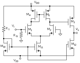
Also, M11 and M12 are referred to the same reference voltage such that
Equation 14.25
![]()
Using ID3 = ID12 and ID11 = 2ID5, we obtain
Equation 14.26
![]()
Combining ( ) and ( ) leads to
Equation 14.27
![]()
Assume that W11 has been picked to satisfy the design ID11. W12 is then selected to give the design ID12 using ID12/ID10 = W12/W10. W5 is selected on the basis of signal considerations. This leaves the computation of W3 [from (
A precision calculation includes the lambda effects and is from
Equation 14.28
![]()
The simple form should normally suffice. The dc output voltage VO is very sensitive to some of the parameters and the approximate calculation from ( ) will not result in VO = 0. However, uncertainties in transistor parameters preclude the justification of using ( ) in practice.
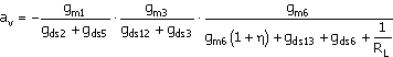
The overall signal gain is now obtainable using ( ) for the differential stage and ( ) for the common-source stage with a current-source load. The result is
Equation 14.29
![]()
A useful form for making a quantitative gain assessment is
Equation 14.30
![]()
Based on the same parameters as used previously for gain calculations (ln lp = 1/20 V and Veffn = Veffp = 0.3 V), the gain magnitude is 4440. The value compares with 116 for the all-resistor circuit for Fig. 13.1 and 289 for the circuit of Fig. 14.3. In this special case, both stages contribute the same value.
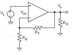
It is evident from the gain result, ( ), that the high gain depends on having a high resistance at the output; a relatively small load resistor can reduce the gain substantially. For example, suppose that the amplifier is to be used as a resistance feedback amplifier as shown in Fig. 14.6. The input is at the gate of M2, and the feedback resistor is connected back to the gate of M1. The load at the output is Rf + R2 || RO.
For a specific example, assume that RO >> Rf >> R2 such that the load is approximately Rf. With the additional load, the gain (14.30) becomes
Equation 14.31
![]()
which is the result of Rf being in parallel with the output resistance of the common-source stage. Suppose that Rf = 10 kW and ID3 = 100 mA. In this case the gain would drop to about 400 (from about 4400), which would be unacceptable, as proper operation of opamps assumes a very high gain.
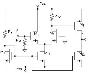
This loading problem is substantially eliminated with the addition of a buffer stage to isolate the load from the output node of the common-source stage, as shown in the circuit of Fig. 14.7. The source-follower buffer stage is made up of M6 and M13. The current-source bias transistor M13 also uses the reference voltage provided by M10. The load on the common-source stage of M3 is now infinite. The feedback network is included in the circuit for comparing with the diagrammatic version of the circuit of Fig. 14.6
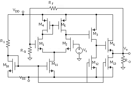
The gain expression of the source follower requires that the body effect be taken into consideration, as the body of M6 will be at signal ground. [The body of M6 will be attached to the negative supply voltage (not shown).] From Unit 7 it was shown that the source-follower stage gain, with resistor bias [( )] for this case is
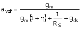
For the present case of current-source bias for the source-follower stage, the gain expression becomes, with inclusion now of the feedback network and the external load resistance of Fig. 14.7
Equation 14.32

To obtain a
quantitative sense of the body effect on the gain of the source follower,
suppose that h = 0.15. Thus, in the limit for gm6
![]()
![]() , avsf = 0.87. This is the best possible result, given the
body effect.
, avsf = 0.87. This is the best possible result, given the
body effect.
For a more general assessment, we can substitute the relations gm = 2ID/Veff, [( )], and gds = IDln )] into ( ) to obtain
Equation 14.33
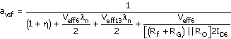
We note that the terms associated with gds6 and gds13 are negligible. Minimization of the resistance term requires making gm6[(Rf + R2) || RO] >> 1 (making the output resistance of the source follower much less than the load resistance). This involves a combination of a large ID6 and kn6.
Suppose that ID6 = 400 mA, W6 = 500 mm, KPn = 100 mA/V2, and that the gate length is L = 10 mm. Recalling that kn = (KPn/2)(W/L) (Table 3.1), we obtain kn = 2500 mA/V2 and 1/gm6 = 500 W. Thus, for example, for RO = 10 kW, Rf = 10 kW, and Rf >> RG, avsf = 0.80, compared with the limiting value of avsf = 0.87. Thus the source follower functions very well to isolate the load from the high-gain common-source stage.
Finally, we write the overall gain expression, including a general load resistance, RL, by combining ( ) and ( ) as
Equation 14.34
A good approximation for the case of a sufficiently large gm6 is
Equation 14.35
![]()
The output resistance of the resistance feedback amplifier was considered in Unit 11.4. There it was shown to be Ro = ro/(1 + T) [( )], where ro is the output resistance of the open-loop amplifier and T is the loop gain of the feedback amplifier. Therefore, with the expectation that T >> 1, the output resistance of the feedback amplifier is very small. For example, consider the amplifier of Fig. 14.7, with no external load on the output and neglecting the effect of the feedback resistors. The open-loop output resistance is
Equation 14.36
![]()
The output resistance of the feedback amplifier is
Equation 14.37
![]()
where the loop gain is T = avoRG/(RG + Rf).
Suppose that in order to get a high gain from the amplifier, we redesign the MOSFETs to have lp ln = 0.01 V-1 for a new av = 96,000 [from ( ), no loading]. Also, let Rf = 10 kW and RG = 100 W. Using the same numbers as in the calculation of a sample source-follower stage gain [( )], ro = 435 W and Ro = 0.45 W
The gain of the feedback amplifier is ( ), which is

with (11.4)
![]()
Here, gain Av is for the case of no external load (including the omission of the load from the feedback resistors). The value is Av = 100.9 for AvNI = 101.
Now we include an external load of RO = 100 W and combine this in parallel with Rf = 10 kW for load RL = 99 W. The loading effect reduces the open-loop gain to av = 18,000. The reduction is all attributed to the loading on the source-follower stage. The amplifier gain [from ( )] is now AvLoad = 100.4. However, with Ro known, an alternative means of obtaining the gain with loading is to use
Equation 14.38
![]()
Av and Ro are calculated once, using ( ) and ( ), respectively. Thus, the effect of loading can be obtained with one calculation using ( ). As in the sample calculation above for the amplifier gain with loading included, AvLoad = 100.4.
The TS271 operational amplifier is designed to operate at very low current levels. This would include the current of the source follower of the output stage. In this case, the output resistance of an amplifier with a simple source-follower stage for an output stage, such as in Fig. 14.7, would be unacceptably high. In the TS271 operational amplifier, the 9-transistor circuit of Fig. 14.8 replaces the simple source-follower stage consisting of M6 and M13 of Fig. 14.7. Note that the circuit of Fig. 14.8 uses different transistor designators. In Fig. 14.7, M6 and M13 are equivalent to M1 and Mn1 of Fig. 14.8
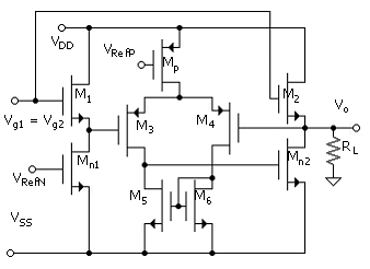
The circuit
of Fig.
14.8
has an additional source-follower stage consisting of M2 and Mn2.
The output from the common-source stage (drain of M3 of Fig.
14.7)
is applied to the gates of both source-follower stages. The sources (outputs)
of M1 and M2 are connected to the inputs of the
differential-stage gates of M3 and M4, respectively.
There is no load at the source of M1 such that the gain of the
source follower can be considered unity. Thus, Vg3 ![]() Vg2 = Vg1 (incremental voltages). By contrast, the
source of M2 is connected to RL such that, in general, Vo
= Vs2 < Vg2.
Vg2 = Vg1 (incremental voltages). By contrast, the
source of M2 is connected to RL such that, in general, Vo
= Vs2 < Vg2.
From another perspective, suppose Vg2 = 1V, that is the source-follower gates are raised by 1V above the bias level. With a load, RL, the current increase will be greater for M2 compared to M1. This will cause the source voltage of M2 to be slightly lower (than that of M1) such that the input to the differential amplifier is nonzero and the output voltage (drain of M3) will drop. The result is a reduction of the gate voltage of Mn2 and thus a reduction of the drain current in Mn2. The incremental drain current of Mn2 provides most of the current through the load; the load current is dominated by the change in the current of Mn2 instead of M2.
Fig. 14.9 is a reasonable equivalent, incremental, circuit. The differential stage (M3, minus, M4, plus, and the drain of M3 as the output) is represented by an opamp symbol.
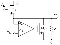
Since the source follower of M1 has a transfer function of nearly unity, incremental Vg2(= Vg1) is moved directly to gate of M3 (minus input of the differential amplifier) as in Fig. 14.9 Thus
Equation 14.39
![]()
where avda is the gain of the opamp and the output of the opamp is Vgsn2. The amplifier (output stage) output voltage is therefore
Equation 14.40
![]()
where we now assume that gm2 = gmn2. It follows that the relation between Vgs2 and Vo is
Equation 14.41
![]()
Combining this with
Equation 14.42
![]()
gives the transfer function, input to output, as
Equation 14.43
![]()
where
Equation 14.44
![]()
The output resistance of the circuit of Fig. 14.8 is 1/Gm. The output resistance of the circuit of Fig. 14.8 is thus reduced by a factor of about 1/avda compared to the circuit of Fig. 14.7 for the same gm of the source follower transistors. From (14.18), the gain of the differential-amplifier stage is
![]()
This would typically be on the order of 100. Thus a significant benefit over the simple source-follower stage output is realized with the circuit of Fig. 14.8. It is also significant that there is no body effect associated with Mn2.
|
|
Bias equation for differential amplifier stage. |
|
|
Differential-stage common-mode gain equation for case of drain bias resistor, RD2. |
|
CMRR = 1 + gm12rds11 |
Common-mode rejection ratio for case of drain bias resistor, RD2. |
|
|
Bias equation for common-source stage. |
|
|
Common-source stage gain with current-source load. |
|
|
Amplifier gain for case of differential-stage drain bias resistor, RD2, and common-source stage gain with current-source load. |
|
|
Output resistance of differential stage with current-source load. |
|
|
Differential-stage gain with current-source load and external load resistor, RL. |
|
|
Relation to determine M3 gate width, W3. |
|
|
Precision relation to determine M3 gate width, RD2. |
|
|
Gain for two-stage amplifier, both stages with current-source loads. |
|
|
Gain of the source-follower stage for the case of load Rf + RG || RO (feedback resistors and external load, Ro). |
|
|
Output resistance of source-follower stage. |
|
|
Output resistance of resistance feedback amplifier |
|
|
TS271 output resistance, where gm2 is for the source-follower stage and avda is the gain of the differential amplifier stage. |
|