PC.1 SPICE Equations and Pin Diagram
PC.2 DC Circuit Setup and Parameter Determination
PC.3 Amplifier Gain at One Bias Current
PC.4 Amplifier Gain versus Bias Current
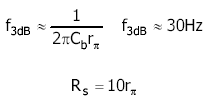
PC.5 Gain-Measurement Frequency Response
Exercises and Analysis ExerciseC1.mcd - ProjectC1.mcd
|
SPICE Equation |
Description |
|
|
|
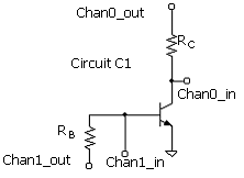
Common Emitter Amplifier with Rc (bias) Load |
|||
|
avb = -gmRC gm = Ic/VT |
C.17 |
Base-to-collector gain. |
|
|
|
C.22 |
Circuit gain with large source resistor. |
|
|
|
C.28 |
Precision base-to-collector gain. |
|
|
|
C.15 |
Transistor input resistance. |
|
|
|
C.40 |
Transistor output resistance. |
|
|
Components
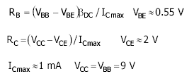
Use ProjectC1.mcd for calculations. Verify bias of Circuit C3 (i.e.VCC < 10 V).
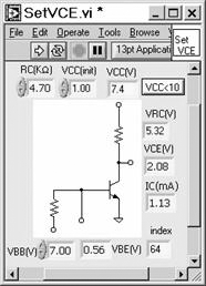
Procedure Type in RC. Run SetVCE.vi while re-adjusting VBB to verify that 0.1 mA<IC<1 mA can be obtained without VCC>10V. VCC is ramped up to obtain VCE=2 V. This will be the operating point (bias) voltage in the gain measurement. Determine VBB for IC=0.1 mA, as in the example. Default and save this in the Front Panel, for use in the next two parts. Now re-run and determine the val 424m1211e ue of VBB corresponding to IC=0.5 mA. This is used in the next step. Circuit C1 is used to obtain dc parameters as in Project B. To obtain a fresh set of parameter values, open subVI IC_VCEsubC.vi. Set in RC and RB and VBB as determined above for IC=0.5 mA. Run the VI. When it has been verified that the VI operates properly, open IC_VCE_C.vi and set in RC and RB and VBB for IC=0.5 mA in the Front Panel of this VI. Run the VI to obtain values for VAF and IS. Get VAF for 1 V<VCE<3 V. Default and save the Front Panel to preserve these numbers. These parameters are also available for Project C2 on the npn - pnp amplifier. |
|
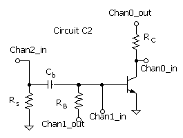
Components Compute Cb for Circuit C3. (Use ProjectC1.mcd.) It will be more than adequate for Circuit C2.
SubVIs SetVSD.vi (Set Bias) FG_10.vi (Function Generator) FG_12.vi (Function Generator) SR_10.vi (Send - Receive Function) SR_12.vi (Send - Receive Function) Oscilloscope_10.vi (Chan0_in) Oscilloscope_12.vi (Chan2_in) LabVIEW Computations
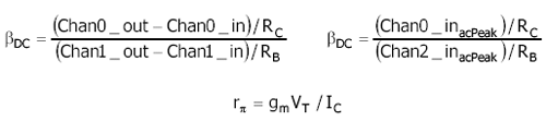
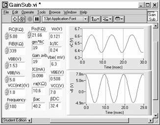
Procedure Connect the additional components in Circuit C2, Rs, and Cb. Connect Chan2_in for reading for reading the base signal voltage. GainSub.vi sends out bias and signal voltage (Chan1_out). (The signal is superimposed on the bias; the bias is modulated with signal.) Chan0_in reads the response (output of amplifier). The VI then resends the input signal (Chan1_out) and reads the response at the base (Chan2_in). These results are displayed in the two graphs. The ac peak values are used to calculate the gain. The VI also computes and displays rp bDC, and bac.
Open GainSub.vi. Set the Digital Controls for collector resistor, RC, base resistor, RB, and Rs. Rs is used to compute the signal current through Rs. Set Frequency at between 10 and 1000 Hz. Set VBB for 0.1 mA as determined with SetVCE.vi. VCC(init) must be less than or equal to 2 V. Default the Front Panel to hold these values for when GainSub.vi is used as a subVI. Ratio VBB/Vs is set at 5. The VI uses this to set Vs = VBB/5, producing, roughly, IB/Ib = 5. This results from IB = (VBB - VBE)/RB and Ib = Vs/RB. This current ratio provides for operation in the linear mode. Run GainSub.vi and verify IC |
|
Procedure Gain.vi is the main VI that obtains the voltage gain as a function of collector bias current. Open Gain.vi and verify that VBB(init) is set to your value for IC=0.1 mA and VBB/Vs=5. VCC(init) will be forced to 1 V in the execution of Gain.vi. Keep subVI GainSub.vi open to help observe the measurement in progress and to obtain Front Panel information for the maximum current. Verify that the correct data are defaulted in the Front Panel of GainSub.vi. The resistors values are not reset in the top VI. Open 5COLDATA.vi. Open
Run Gain.vi to obtain the gain for a range of collector
current with maximum IC The data file includes results for IC, avb, bDC, and bac and rp. The data provide for making a comparison between measured data and SPICE computations in the Mathcad project file. Default and save the Front Panel of 5COLDATA.vi for a data file backup. Default the Front Panel of Gain.vi to save the value of VBB for the maximum current. Default and save the Front Panel of GainSub.vi to save the value of VBE at the maximum current. For obtaining a file from the saved data in Gain.vi, use GainData.vi. Transfer the data from the three Indicator Graphs of Gain.vi to the three equivalent Control Graphs in GainData.vi. Run GainData.vi to obtain the data file. |
|
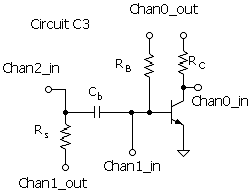
Procedure Circuit C3 has the input signal applied through the coupling capacitor. Chan0_out V(CCV) provides the input and output circuit bias. The base signal with dc removed is measured again with Chan2_in. Reconnect the circuit according to Circuit C3. Connect the top of RB to Chan2_out and the bottom of Rs to Chan2_out. Open SetVCEC3.vi and run to determine circuit bias IC and VCC.
Note that if VCC > 10 with VCE < 2 V, a smaller value of RC or larger value of RB is required; that is,
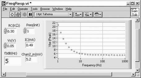
there is not a valid solution. (If VCE The VI for the frequency-response measurement is FreqResp.vi (below). The VI sends out a signal through out Chan1_out over the frequency range of) Freq(init) to 1 kHz. The response at the base input node on the source side of the capacitor is measured with in Chan2_in as in Circuit C2. Open FreqResp.vi and install your
value of RC in the Front Panel. Select Vs such as to obtain Vbe Open subVI FG1Chan.vi to monitor the waveform of the signal from in Chan2_in. Keep SetVCEC3.vi open to verify that the dc setup functions properly. Note that the dc setup process is configured to be slow to allow the capacitor transient to be completed.
Run FreqResp.vi. Verify that in Chan2_in (ac peak) is about 5 to 10 mV at the highest frequency. Adjust Vs accordingly. Verify that a flat response is obtained at the higher frequencies. If not, a larger capacitor is needed. Default and save the Front Panel to preserve the f3dB information. From the ProjectC1.llb, open XYToDataFile.vi. Copy and paste the graph data to obtain a frequency-response data set. |
|