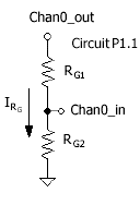
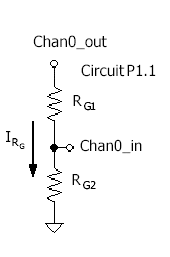
P1.1 Resistor Voltage-Divider Measurements
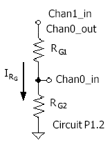
P1.2 Resistor Voltage Divider with Current Measurement
P1.3 Resistor Voltage Divider with Resistor Measurement
P1.4 Resistor Voltage Divider with a Sine-Wave Source Voltage
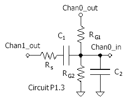
P1.5 Frequency Response of a Resistor-Capacitor Circuit
Exercises and Analysis Exercise01.mcd - Project01.mcd
|
Components
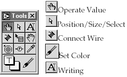
Programming Exercise 1.1 Use Tab to switch between Tools. Use Space Bar to switch between Wiring Tool and Position Tool (arrow). Get Tools Palette under Windows menu (or Shift/Right Click) from the Diagram.
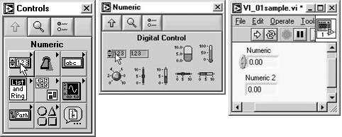
Open a new VI to construct your VI_01.vi.
The VI opens with a Front Panel (top) and a Diagram (under). Switch from one
to the other using the Windows menu or Ctrl/E. The VI opens with the Operate
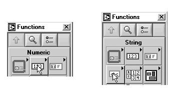
Value Tool Place a Digital Control and Digital Indicator on the Front Panel 18118x2322s (example below). (Right Click on Front Panel to get the Controls Palette.) The Digital Control and Digital Indicator are in the Numeric Palette (below). Save the file with your choice of Name.
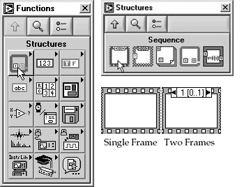
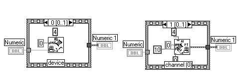
Go to the Diagram (Ctrl/E) or Window>>Show Diagram. Place a Sequence Structure in the Diagram. (Right Click on Diagram to get Functions>>Structures>>Sequence Structure.) Enlarge the Structure by contacting the Arrow Tool (Position Tool) at the bottom-right corner of the Structure (drag).
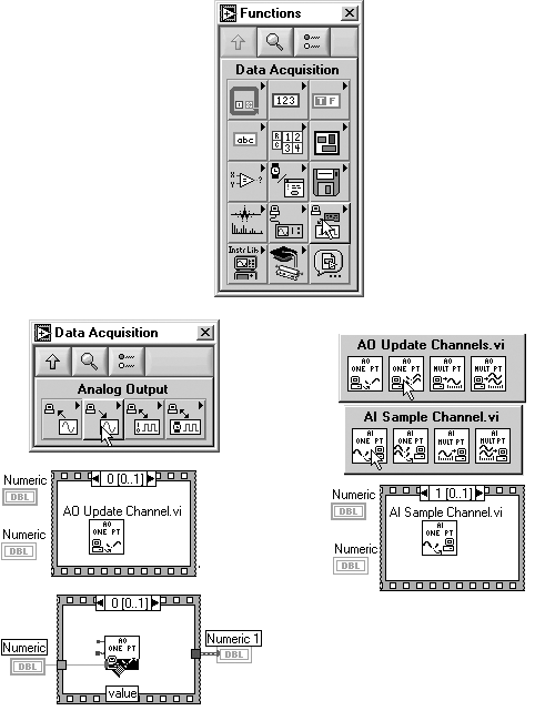
Right Click on the edge of the Frame and Add Frame After. Click on arrows to switch between Frame 0 and Frame 1. Place AO Update Channel.vi in Frame 0. (Functions>>Data Acquisition>>Analog Output >>AO Update Channel.vi.) Place AI Sample Channel.vi in Frame 1. (Functions>>Data Acquisition>>Analog Input>>AI Sample Channel.vi.)
Position the icons, etc., with the Arrow Tool (Left Click>>Drag). Wire the Digital Control (darker) terminal to the value terminal of the Analog Output VI, AO Update Channel.vi. Press the space bar to alternate between the Wiring Tool and Position (arrow) Tool. To wire, get the Wiring Tool (space bar), Left Click on a terminal, release, drag the Tool to the opposite terminal, and Left Click. To clean up wiring mistakes, use Ctrl/B. Note that the terminal name (value in the example) of an icon is displayed while the Wiring Tool is over the terminal.
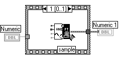
Wire the Digital Indicator terminal (lighter) to the output terminal (sample) of the Analog Input VI, AI Sample Channel.vi. Place the Constant (4) and the String (0) in the Diagram as shown in the example (Frame 0). Use the Writing Tool to type in the numbers. The location of Constants and Strings, under Functions, is shown below. Place Constants (4), (10) and (0) and String (0) in Frame 1.
Wire the Constants and Strings as shown in the examples. To wire, get the Wiring Tool (space bar), Left Click on a terminal, release, drag the Tool to the opposite terminal, and Left Click. To clean up wiring mistakes, use Ctrl/B.
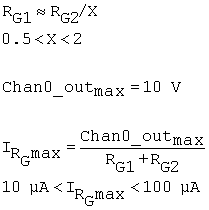
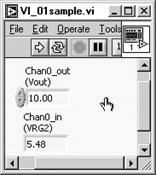
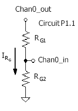
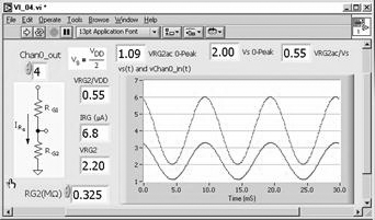
Change the names of the Digital Control and Digital Indicator. Use the Writing Tool. This can be done from the Diagram or the Front Panel. Click on the existing name (e.g., Numeric) and edit. Procedure Calculate the resistor values. Connect the circuit. To Run a VI, from the Front Panel, use Operate>>Run or (better) use Ctrl/R. Run the VI with Chan0_out = 10V (Vout) and note the value of Chan0_in (VRG2). This should be consistent with your resistor ratio choice. Try a variety of Chan0_out values. (The maximum is 10 V.)
(Optional) To install the circuit Diagram on the Front Panel 18118x2322s , open VI_01.vi from Project01.llb. Use the Arrow Tool, Click on the circuit diagram, use Window's copy (Ctrl/C), and paste it into you VI Front Panel. |
|
LabVIEW Computation
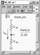
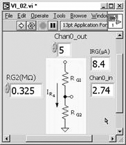
Programming Exercise 1.2 Save a copy of VI_01.vi (your name) and give it a new name (such as #2). On the Front Panel 18118x2322s , place a Digital Indicator for IRG (Controls>>Numeric). On the Front Panel 18118x2322s , place a Digital Control for the resistor value. (Controls>>Numeric.) In the Diagram (below) place a Divide operation. (Functions>>Numeric>>Divide.) Wire the Diagram as in the example.
Procedure Set your value of RG2 in the Digital Control (MW). To set in three digits, change the precision. Right Click on the Control, go to Format and Precision, and change Digits of Precision.
Run VI_02.vi with Chan0_out set at 5 V and note the value of IRG. Default and save the Front Panel for comparison with the Mathcad evaluation file. For Default, menu Operate>>Make Current Values Default. |
|
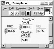
Basic sample shown below.
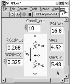
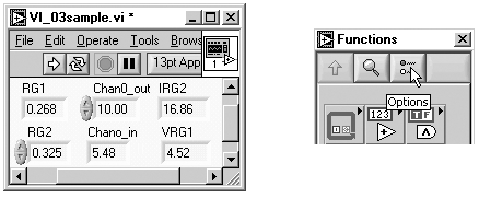
Programming Exercise 1.3 Save a copy of VI_02.vi with a new name and add Digital Indicators for VRG1 and RG1 as in VI_03.vi (basic sample below). The new VI will find and indicate the value of RG1.
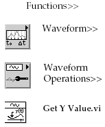
In the Diagram, we will add Get Y Value.vi. This VI is found in the Functions Palette with the sequence shown on the left. Note that the full Palette Set is required. Your Palette may be an abbreviated form called Basic. If so, open the Palette and use the Stick Pin to keep it open. Then Click on Options as shown below. Select the default Palette Set.
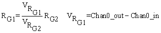
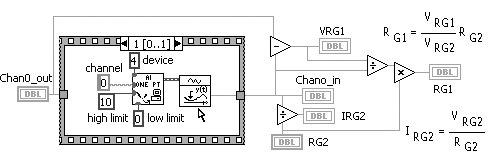
Get Y Value.vi is used to extract a given Y value in a waveform. AI Sample Channel.vi is a special case of a waveform with only one component. In the VI of part P1.2, we connected the output directly to a Digital Indicator, in which case, LabVIEW sorted out the component value automatically. Place Get Y Value.vi as shown in the Diagram (cursor, Arrow). Connect the balance of the circuit as shown. The new math formulations are indicated below and in the Diagram. LabVIEW Computations
Procedure Run the VI_03.vi for Chan0_out set at 10 V. Note the value of RG1 and VRG1. Default and save the Front Panel for the Mathcad evaluation file. |
|
Procedure The VI sends out, on Chan0_out, a sine-wave superimposed on the dc value. Add the connection, Chan1_in, directly to the output channel. Run the VI for various values of Chan0_out. Note that the maximum allowed Chan0_out is about 6 V since the dc and ac peak must be less than 10 V. Verify that the results are consistent. For example, the peak ac values must be 1.5 of the dc values since Vs = VDD/2. Default and save the Front Panel using Chan0_out = 4V. |
|
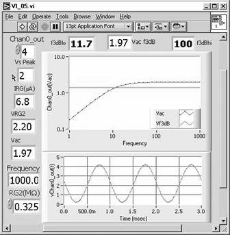
Components C1 = C2 f3dBhi = 50f3dBlo Rs f3dBlo = 5 Hz (approximately)
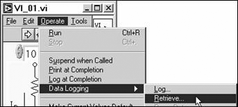
Typical C1 Procedure Configure the circuit for the low-end measurement and f3dBlo. Install C1 and do not install C2. Run VI_05.vi to obtain f3dBlo. Obtain a Log of the Front Panel to save the results. To obtain a Log, go through menu sequence Operate>>Data Logging>>Log. To retrieve data: Operate>>Data Logging>>Retrieve. An example of retrieving a Log using VI_01.vi is shown here. Note that at the first Data Logging, you will be asked to name a Data Log file. Select any name and Click Save, to install Log File in the Project folder.
Now move the capacitor C2 = C1 to the C2 location and install a large capacitor, C1new, in place of C1, which satisfies C1new >> C2 (e.g., C1new = 47 mF). Note that the source side of the capacitor (connected to Rs) is more negative than the output side (Chan0_in). Run VI_05.vi to obtain f3dBhi. Default and save the Front Panel. Note that when reopening the VI, the Front Panel will contain the information last defaulted from this f3dBhi measurement. The first measurement is in the data Log. Repeating, to retrieve the information from the data Log, go through menu sequence Operate>>Data Logging>>Retrieve. To then go back to the defaulted Front Panel, click OK and go through Operate>>Reinitialize All to Default Values. Note that if C2 = C1 are actually both in the circuit at the same time, the output in the plateau region is 1/2 as large (Exercise 1). This configuration is not implemented here. The use of C2 = C1 is only for convenience and f3dBlo << f3dBhi is satisfied with Rs << RG.
|
|