Analog amplifier stages (BJT) generally comprise three possible terminal configurations: common emitter, common base, and common collector (emitter follower). As the names suggest, in each case, the input and output are referred to the common terminal. The MOSFET equivalents are common source, common gate, and common drain (source follower), respectively.
As the most fundamental of transistor amplifier building blocks, the common-emitter stage is the logical configuration to begin a study of signal amplifiers. The common-emitter considered initially in this unit is obtainable with a simple extension of the dc measurement circuit from Unit B Fig. B.12). Based on this circuit various aspects germane to signal amplifiers in general are discussed. In Unit C.7, the common-emitter stage with active load is explored. Both types of amplifiers, with resistive and active 22422y2416w loads, are investigated extensively in projects.
The emitter-follower stage is discussed in Unit C.9 along with a general treatment of the various effects on the common-emitter stage with an emitter-branch resistor. An entire unit (Unit C.7) is devoted to the source-follower stage, the MOSFET equivalent of the emitter-follower stage. The common-gate stage, the MOSFET equivalent of the BJT common-base stage, is considered extensively in conjunction with the role it plays in the differential amplifier stage (Unit 8
The two common-emitter amplifier-stage configurations studied in projects are shown in Fig. C.1. We note that the dc circuit of Fig. C.1(a) is that of Fig. B.12. Amplifier performance analysis can be performed with the two output channels available from the DAQ in the following manner: Fig. C.1(a) uses separate channels for the input and output bias circuits and superimposes the input signal on the input bias. In Fig. C.1(b) we add a signal-source resistor and coupling capacitor and use one channel for the input signal and one channel for bias. The capacitor is required to prevent the connection of the signal source from affecting the dc (bias) operation of the circuit. The latter represents the classical practical common-emitter amplifier stage. The signal-source resistor provides for a current-source input signal and hence linear amplification.
In the experimental project on the common-emitter amplifiers, we measure the voltage gain as a function of the collector current and compare the results with SPICE. The bias collector current is swept from 0.1 to 1 mA. The measurement uses the circuit in Fig. C.1(a). A DAQ output channel (VBB) sets the bias currents. Another output channel (VCC) sets the design bias VCE at each bias current. The gain of the circuit of Fig. C.1(b) is also measured with particular emphasis on the bias solution and the frequency response.
A formulation for obtaining the collector current for a given VBB [Fig. C.1(a)] is based on the following: From the input loop equation,
Equation C.1
![]()
The two relevant transistor characterization equations are (B.6
![]()
and base - emitter dc voltage equation, from (B.7), setting VBC = 0 for simplicity,
Equation C.2
The equation set above has three unknowns, IC, IB, and VBE. The equations can be combined to obtain a function for IC,
Equation C.3
A good
estimate can be obtained with using VBE ![]() 0.6 V, giving simply
0.6 V, giving simply
Equation C.4
![]()
The simple expression is sufficient, for example, for selecting a value for RB in the circuit of Fig. C.1(a) in the BJT amplifier project. We have also neglected the dependence of bDC on VBC of (B.11). This is a reasonable approximation for establishing the nominal values for the measurement circuit components.
The collector - emitter voltage, VCE, is then established with
Equation C.5
![]()
In designing a project circuit for a current sweep, RB and RC are selected for the highest currents and highest DAQ output voltage. In the amplifier project, the circuit of Fig. C.1(b) uses the resistors from the circuit of Fig. C.1(a). It thus has a unique bias variable and VCC solution for a given design VCE requirement. This is based on (C.3) and (C.5) and is
Equation C.6
![]()
In the amplifier project, the project Mathcad file is used to find the solution for VCC [with an educated guess for VBE, as in (C.4)]. If the result has VCC > 10 V, the limit from the DAQ, it is necessary to decrease RC or increase RB. This may be necessary, as the transistor bDC is not known with precision at the point of the selection of the resistor values. After measuring the actual VCC, the result is used in the Mathcad file to compute a value for bDC from a circuit solution.
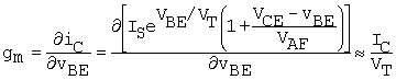
The primary function of a transistor in analog circuits is to produce a signal output current in response to a signal input voltage. In the case of the common-emitter circuits of Fig. C.1, the transistor input voltage is Vbe and the responding output current is the collector current Ic. (Variable subscript conventions are covered in Unit 2. Uppercase symbols with lowercase subscripts denote RMS or peak magnitude of periodic signals.) The linear relation between the two variables is the transconductance, gm. By definition, for the BJT
Equation C.7
![]()
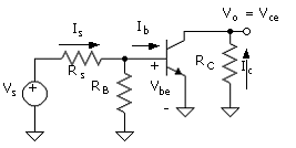
In some simple amplifier circuits, this would be all that would have to be known about the transistor to perform a design or analysis. More generally, however, the model also includes input and output resistances, ri = rb + rp and ro, respectively. The transistor linear model, which includes these components and a load resistor (in this case, bias resistor, RC), is shown in Fig. C.2. Applied input voltage Vbe and responding Ic are indicated.
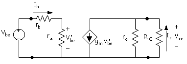
The input resistance relates the input signal base current Ib to the signal emitter - base voltage, Vbe, that is
Equation C.8
![]()
Parameter rb
is the actual physical resistance through which the base current must flow to
arrive at the true, internal physical base - emitter junction. The signal
voltage across the internal base - emitter junction is ![]() . Parameter rp is the linear relation between Ib
and
. Parameter rp is the linear relation between Ib
and ![]() and is not a physical resistance.
and is not a physical resistance.
We assume in
the following discussion that rp
>> rb. This is especially true in the low current range of our
BJT transistor projects. As will be seen below, rp is inversely proportional to bias collector current, IC,
whereas rb is close to a constant and could be significant at
currents corresponding to midrange or higher for the transistor. (As a rule, rb
must be taken into consideration when the model is applied in very high
frequency applications.) Note that neglecting rb compared to rp is equivalent to ![]() , as assumed below.
, as assumed below.
The output-resistance parameter, ro, accounts for the fact that total collector current, iC, increases with increasing total collector - emitter voltage, vCE. According to the output resistance parameter relationship, the current through this resistance is
Equation C.9
![]()
Including ro, the current through the load, in this case bias resistor, RC, is
Equation C.10
![]()
This current flows up through RC such that Vce is negative for positive Vbe. Thus, the current associated with ro subtracts from gmVbe to reduce the current through RC. For a positive Vbe, there is an increase in the total vBE, thus causing the total collector current to increase. The result is a decrease in the total vCE and hence a negative incremental Vce.
The two components of (C.10) are illustrated graphically in Fig. C.3. The output characteristics are for two values of base - emitter voltage: bias only, VBE, and bias plus base - emitter signal voltage, VBE + Vbe. They are designated Bias and Signal. The solution to iC and vCE is constrained to the "load line," which is iRc = iC = VCC/RC - vCE/RC [(C.5
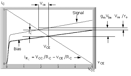
At a constant vCE = VCE, the change in the current-source current for the applied Vbe is gmVbe [(C.7)]. The net collector current change (signal current), Ic, though, is as given by (C.10); that is, it includes the component associated with ro. Since the output characteristic slopes downward for decreasing vCE, the actual transconductance decreases, but the linear model treats this effect with a constant gm combined with the effect of the output resistance, ro.
We can relate the values of the two parameters in (C.10) to the SPICE model parameters using (B.7) with the substitution vBC = -(vCE - vBE). This is
Equation C.11
Differentiating (C.11) with respect to vBE (with vCE = VCE, Vce = 0), gm is found to be
Equation C.12
The approximate form only ignores a term on the order of IC/VAF, where VAF >> VT.
The output resistance is obtained with vBE = VBE (bias value) or Vbe = 0. This is
Equation C.13
![]()
where, from (C.11), IC(vCE = VBE) = ISexp(VBE/VT). For simplicity, the bias collector current, from (C.11), IC = iC(VCE), is usually used for the calculation for ro. Finally, a relation for rp comes directly from (C.7), Ic = gmVbe, and (B.41), Ic = bacIb. Equating the two gives
Equation C.14
![]()
Hence, from
the definition rp = Vbe/Ib
(with ![]()
Equation C.15
![]()
Note that the right-hand side of (C.14) is the alternative current-dependent current source of the linear model of Fig. C.2
As discussed in Unit B.9 bac can be slightly different from bDC, but the distinction usually need not be made in analysis or design. This is due to the fact that bDC tends to be quite variable among devices and that most analog designs are based on making the results as independent of bDC as possible. Signal parameter bac will be used in the following, but it is understood that bDC can be used in the calculations without serious penalty in precision.
Any transistor amplifier stage has a gain from the input terminal to its output terminal (base and collector, respectively, for this case). But the circuit gain, from the source to the output, takes into consideration the possible finite input resistance at the transistor input terminal. Due to the finite signal-source resistance, an attenuation results from the signal-source to the transistor input terminal. The example of this case of the common-emitter amplifier stage is considered here.
The midband (frequency-independent) signal version of the circuit of Fig. C.1(b) is shown in Fig. C.4. It is obtained from the general circuit by converting dc voltages to zero. This includes the capacitor voltage, which ideally, remains at its constant dc (bias) value. The rule followed here is that if there is no incremental variation between any two nodes with a signal applied at the input, then the component between the two nodes is superfluous. In Fig. C.4, the output voltage is Vo = Vce and the signal source is designated Vs along with its source resistance, Rs. In the case of an actual signal source, Rs is probably an equivalent rather than an actual resistor. Thus, it is assigned a lowercase subscript.
Neglecting the output resistance, the signal collector current for a signal voltage applied at the base reverts to (C.7), which is
![]()
with gm = IC/VT [(C.12)]. IC is the bias current with uppercase subscript, not the signal, with lowercase subscript. (Recall that signal voltage and currents can be, for example, periodic peak or RMS values or instantaneous values, as these are all proportional throughout the linear circuit. To be specific, as in the experiment on the common-emitter amplifier, we consider them to be periodic-signal peak values.)
The signal voltage developed at the collector is (still assuming that ro >> RC)
Equation C.16
![]()
From (C.16) and (C.7), the gain of the transistor in the circuit (input at the base of the transistor and output at the collector) is
Equation C.17
![]()
We note that the magnitude of the result is the dc voltage drop across the bias resistor divided by VT. For example, for VRc = 5 V and VT = 26 mV (room temperature), the gain magnitude is about 200. The BJT circuit is capable of providing very substantial voltage gains.
The circuit input resistance looking into the base of the transistor, Rb, is the transistor input resistance, rp (still neglecting rb), in parallel with the bias resistor RB, that is,
Equation C.18
![]()
The gain from the signal source to the output at the collector of the transistor is thus
Equation C.19
![]()
When the input-signal source resistance is large (Rs >> Rb), a good approximation for av is
Equation C.20
![]()
Further approximation can be made using RB >> rp, to obtain
Equation C.21
![]()
Finally, using bac = gmrp C.15
Equation C.22
![]()
This result
is intuitive on the basis of Ib ![]() Is, Is
Is, Is ![]() Vs/Rs, and Ic
= bacIb. The sequence of approximations
for the gain magnitude is
Vs/Rs, and Ic
= bacIb. The sequence of approximations
for the gain magnitude is
Equation C.23
![]()
An additional
approximation is with bac ![]() bDC
bDC
Note that the requirement for the voltage gain to be greater than unity is that Rs < bacRC. Thus, for sources with a large Rs, an amplifier design should have a high input resistance stage such as an emitter-follower stage. The emitter-follower stage is discussed in Unit C.9
In the Project
C1
the gain of the amplifier as a function of bias current, IC, is
measured using the circuit of Fig.
C.1(a).
This is made possible with the use of LabVIEW and the DAQ, with two output
channels, to provide a signal source superimposed on the input bias voltage. In
this case, the overall gain from the signal source is restricted (input bias
and signal source resistor are the same) and av ![]() –bacRC/RB. Since RB
of the circuit is roughly bDCRC, the gain is on the order of
unity.
–bacRC/RB. Since RB
of the circuit is roughly bDCRC, the gain is on the order of
unity.
We want now to consider the measurement of the gain of the transistor amplifier (Fig. C.1) based on the linear model. This model is not valid if the signals are too large, such as to cause an unacceptable degree of nonlinearity. If the linear model is valid, the signal input voltage magnitude, between the base and emitter of the transistor, is related to the fraction Ic/IC according to [combining (C.7) and (C.12
Equation C.24
![]()
This voltage must be large enough for a good measurement using the DAQ board in the computer (i.e., at least a few millivolts), yet small enough so as not to cause substantial nonlinearity, which would invalidate the measurement of signal gain. Again, the signal-gain concept is based on the linear model. In the following, we will find the conditions under which the linear model is valid and to what extent.
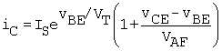
The general expression (active region) between total collector current and total base - emitter voltage, vBE = VBE + Vbe, is (neglecting the VAF factor) [from (B.7
Equation C.25
![]()
or
Equation C.26
where the limit form for |Ic/IC|<<1 gives (C.24). The plus sign is for Ic and Vbe positive, and vice versa.
Since the signal output voltage is Vo = -IcRC, the signal "gain" is
Equation C.27
which reduces to the linear form, (C.17), when |Ic/IC|<<1.
In the
amplifier project, the gain is obtained by dividing the measured signal Vo
by the measured signal Vbe. The circuit has Rs (=RB)
>> rp, such that Ic ![]() bacVs/Rs [as in (C.23)]. As a result, for the positive
and negative peaks of Vs, the positive and negative peak magnitudes
of Ic are equal. Thus, the fraction |Ic/IC| is
the same for both signal polarities. Incremental voltage Vbe will
respond nonsymmetrically according to (C.26). We note that this does not
constitute a form of distortion at the output, as is evident from the
approximate form of (C.23) (neglecting a very small effect
due to variation of bac
bacVs/Rs [as in (C.23)]. As a result, for the positive
and negative peaks of Vs, the positive and negative peak magnitudes
of Ic are equal. Thus, the fraction |Ic/IC| is
the same for both signal polarities. Incremental voltage Vbe will
respond nonsymmetrically according to (C.26). We note that this does not
constitute a form of distortion at the output, as is evident from the
approximate form of (C.23) (neglecting a very small effect
due to variation of bac
For output currents on the order of, for example, |Ic/IC| = 0.5, the plus and minus peak values of Vbe are significantly different. In the amplifier-gain measurement project, the ac voltmeter indicates a peak voltage, which is the average of the plus and minus peak values. To some extent, in this manner, the error is canceled. A comparison is made of the average value of the peaks, Vbeavg, with the distortion-free Vbe, as shown in Fig. C.5
In the
amplifier project, the measurement base - emitter voltage is limited to about
|Ic/IC| = 0.2. This corresponds to Vbe ![]() 5 mV. The measurement error, due to
the distortion discussed here, is only about 1% for this case.
5 mV. The measurement error, due to
the distortion discussed here, is only about 1% for this case.
The
measurement circuit is configured to be able to measure the signal voltage with
the dc base - emitter voltage removed. Therefore, the DAQ conversion limit can
be set at the minimum of 50 mV, where the resolution is much less than Vbe
![]() 5 mV.
5 mV.
As noted, a possible nonlinearity in bac could be a contributor to nonlinearity in the gain function (C.22). The effect from including the bac nonlinearity in the development of (C.27) is also, to a degree, canceled in the averaging process of measuring the gain.
As discussed in Unit C.2, the signal model contains an output resistance, which reflects the fact that the output characteristic of the transistor has a finite slope. This is characterized with the SPICE parameter VAF. It was noted that the effect of the finite slope is to place a resistance effectively across the output of the amplifier. It is calculated from ro = VAF/IC, (C.13
With increasing bias current, ro may not be negligible compared to RC. In the project on the gain of the amplifier, we will read the experimental data into a Mathcad file and adjust VAF to make the SPICE calculation and measured data match. The gain expression that includes transistor output resistance is
Equation C.28
In a
representative transistor, VAF ![]() 100. The circuit design could call
for ICRC
100. The circuit design could call
for ICRC ![]() 5 V for a 10-V supply voltage. In
this case, the output resistance has about a 5% effect on the gain value.
5 V for a 10-V supply voltage. In
this case, the output resistance has about a 5% effect on the gain value.
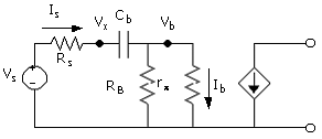
External capacitors are added to the circuits of this unit for two purposes. One, shown in Fig. C.1(b), is to connect the signal input source to the amplifier. The other is a special-purpose capacitor of the amplifier project. It is attached to facilitate measurement of the base - emitter voltage with high resolution. Design considerations for selection of the capacitor values are discussed in the following.
The linear equivalent circuit of the amplifier of Fig. C.1(b) is shown in Fig. C.6. The selection of the value of the capacitor Cb is based on the requirement that it has negligible effect on the signal current at any frequency at which the amplifier will be operated. Including the reactance of the capacitor, the input signal current is
Equation C.29
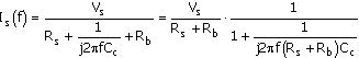
The input signal current magnitude is
Equation C.30
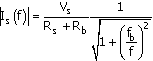
where
Equation C.31
![]()
Frequency f3dB is defined as the frequency where the response magnitude is
Equation C.32
![]()
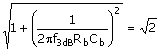
It follows that for this case, f3dB = fb. Note that at f = 10f3dB,
![]()
In Project
C1
measurement of the base input voltage is made at the signal side of the
coupling capacitor. This is the node designated by Vx in Fig.
C.6.
Good measurement precision is provided, as the dc component of the base voltage
is blocked by the coupling capacitor. The maximum voltage sensed by the input
channel is only the signal voltage Vb ![]() Vx
Vx ![]() 5 mV, as discussed in Unit
C.4.
This value is much smaller than dc VBE
5 mV, as discussed in Unit
C.4.
This value is much smaller than dc VBE ![]() 0.5 V. In this configuration, the
limit setting for the input channel is set at 0.1 V, for a resolution of about
48 mV with the input channel in the bipolar mode.
If the peak signal voltage is, for example 5 mV, the resolution is about 1% of
the measured voltage
0.5 V. In this configuration, the
limit setting for the input channel is set at 0.1 V, for a resolution of about
48 mV with the input channel in the bipolar mode.
If the peak signal voltage is, for example 5 mV, the resolution is about 1% of
the measured voltage
The required
capacitor, Cb, for this case and for same f3dB, is
substantially larger than that obtained from (C.31). As will be shown, at f ![]() f3dB, the requirement is
that |XCb|
f3dB, the requirement is
that |XCb| ![]() rp. It follows that at f near f3dB, Rs >> |XCb|
since Rs >> Rb
rp. It follows that at f near f3dB, Rs >> |XCb|
since Rs >> Rb ![]() rp. The input signal current is thus given approximately by
rp. The input signal current is thus given approximately by
Equation C.33
![]()
This includes
the good assumption that Rs >> Rb and that, by
design, |XCb| ![]() Rb for f
Rb for f ![]() f3dB. (Technically, the
pole of the transfer function is ignored.)
f3dB. (Technically, the
pole of the transfer function is ignored.)
The signal voltage, Vx(f), at the input signal source side of the capacitor is the sum of the voltage at the base plus the voltage across the capacitor, that is, with (C.33
Equation C.34
![]()
The ratio Vx(f)/Vb is thus
Equation C.35
![]()
Note that the
form of Vx(f) is falling, for increasing frequencies, to a plateau
(Vb). We will define f3dB as the frequency where the
magnitude of this ratio is ![]() . This could qualify as a type of corner frequency, as it represents the frequency
where the frequency response function is
. This could qualify as a type of corner frequency, as it represents the frequency
where the frequency response function is ![]() times the asymptotic value. A solution for f3dB then comes from
times the asymptotic value. A solution for f3dB then comes from
Equation C.36
giving
Equation C.37
![]()
At f=10f3dB, Vx = 1.005Vb. Note that for this case of a current source [(C.33)], the value of the capacitor can be obtained simply to satisfy |XCb| = rp
The project circuit for making a precision measurement of the gain of the amplifier of Fig. C.1(a) is shown in Fig. C.7. The circuit has the addition of Cb and Rs for measuring the base signal voltage without the dc component. The selection of Rs in the amplifier project is made to satisfy if Rs >> rp such that the effect on the gain referred to Vs is small. The choice is, on the other side, Rs < RB, such that the charging time of Cb is not prohibitively long during the bias sweeps. The f3dB frequency at Vx for this case is (C.31) with fb = f3dB. In the amplifier project, the capacitor is selected from (C.37) to satisfy the requirement for the amplifier of Fig. C.1(b) using (C.37). The capacitor will thus certainly be adequate for the amplifier of Figs. C.1(a) and C.7
In the early days of electronic amplifiers, the voltage amplification device was, of course, the vacuum tube. It existed in only one polarity configuration, that is, with positive plate (bus or rail) voltage. With the appearance of semiconductor transistors came the availability of the dual set of devices with opposite terminal voltage polarities. This is the case for BJTs, JFETs, and MOSFETs. (Vacuum tubes were implemented in class B amplifiers. The application required a pair of inputs, one 180° out of phase with the other, normally derived from a transformer.)
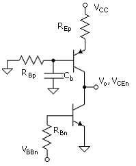
The dual set has provided the versatility for a wide range of electronic system applications, including the amplifier with active load shown in Fig. C.8. This can be compared with the circuit of Fig. C.1, which in place of the pnp transistor, has a bias collector resistor, RC.
Note that either transistor base could serve as the input such that the opposite transistor becomes the load. In Fig. C.8, the npn is chosen as the driver transistor and the pnp as the load transistor.
A dc output characteristic plot is shown in Fig. C.9. Since the collector current of the individual transistors is the same, the solution to bias voltage VCE for the npn is the intersection of the two curves, that is, 5 V. This would be a good choice for a bias output voltage for the power supply voltage of this case, which is 10 V. For the plots, VAFn = 100 V and VAFp = 20 V were used. (In the discussion of the npn - pnp amplifier, the added subscript n or p will denote npn or pnp, respectively.)
A signal impressed at the base of the npn causes the npn curve to move up or down while the pnp curve remains in place. Note that the pnp acts like a load line of a resistive load; however, an extension of the active-region characteristic of the pnp intersects the zero-current axis at VCC + VAFp = 30 V. The pnp active-load transistor thus provides the equivalent of a bias resistor with a power supply of 30 V instead of the actual 10 V.
The gain benefit for the case of the active load is apparent from the following. The equation for the gain of the BJT common-emitter amplifier with resistor RC, which includes the output resistance of the driver transistor (in this case, npn), is a form of (C.28
Equation C.38
where ron is the output resistance of the npn and is given by [generalization of (C.13
Equation C.39
![]()
where VCE and VBE are the transistor bias voltage variables and IC is the collect bias current of the amplifier. Parameters VAFn and VAFp are used in this unit for the slope parameter for the npn and pnp, respectively.
The output resistance expression is generalized here to emphasize that strictly speaking, the collector currents and voltages must match as suggested in the expression. Voltages VBE and VCE are bias values. In the following, as is standard in electronics circuit analysis, we approximate the output resistance, for example, for the npn as follows:
Equation C.40
![]()
It follows that for the pnp
Equation C.41
![]()
where IC
![]() IC(VCE), that
is, the actual bias collector current.
IC(VCE), that
is, the actual bias collector current.
For the pnp active load, the resistor RC is now replaced with the output resistance of the pnp, to obtain
Equation C.42
![]()
where the far right-hand side uses gm = IC/VT.
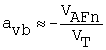
The gains for the resistive load and active load cases can readily be compared with the substitution of gm = IC/VT in (C.38) (gain with load RC) and (C.40) for ron to obtain
Equation C.43
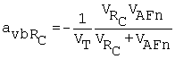
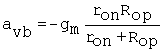
For the example of VCC = 10 V and bias VCE = 5 V, VRc = 5 V. Using VAFn = 100 V and VAFp = 20 V, the room-temperature gain magnitudes are |avbRc| = 4.76 V/0.026 V=183 for the amplifier with Rc load compared to an npn - pnp amplifier gain magnitude of |avb| = 16.7 V/0.026 V=641. In practice, the advantage will be considerably more, as the value for VAFp used here is smaller than normal for BJTs. The small number was used above in the plot (Fig. C.9) to exaggerate the effect of the slope.
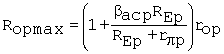
In Project C2 the effect of an emitter resistor in the emitter branch of the pnp, REp, on the output resistance of the pnp will be explored. The circuit is shown in Fig. C.10. The effect of the emitter resistor is to increase the output resistance, due to the negative feedback effect, at the collector of the pnp. This increase can be made to be substantial; in fact, to a good approximation, the load on the amplifier is only ron of the npn.
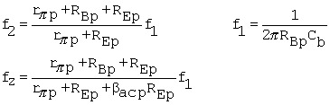
The generalized gain expression, which includes the effect of the emitter resistor, is
Equation C.44
![]()
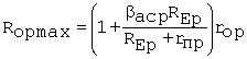
where Rop is the output resistance at the collector of pnp, for the circuit with REp.
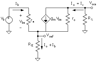
Here, we develop an expression for the output resistance of a BJT with the emitter resistor. This is a function of both REp and RBp. In the Project C2 the amplifier gain is measured with and without a base shunt capacitor, Cb. With the capacitor in place, the base resistance in the signal circuit is effectively zero, and this alters Rop significantly. The linear circuit for the general case of a BJT common-emitter amplifier with emitter resistor is shown in Fig. C.11. The circuit includes a base resistor, RB.
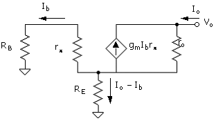
A test voltage, Vo, is applied at the collector with the base resistor and emitter resistor at signal ground. In response, a current Io flows from Vo through RE in parallel with RB + rp. This induces a voltage VRE = (Io - Ib)RE across RE that is applied to rp in series with RB. Base current Ib is a fraction of Io as given by
Equation C.45
Applied voltage Vo sums up to
Equation C.46
![]()
The approximation is based on ro >> RE and is consistent with the fact that the signal voltage drop across the output of the transistor is much greater than across the emitter resistor.
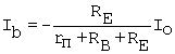
Eliminating Ib in (C.46) using (C.45) results in the solution for Ro, which is
Equation C.47
![]()
The result has two limiting forms based on the relative value of RB: When RB >> rp + RE,
Equation C.48
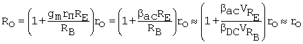
The
approximate form uses IC ![]() IE.
IE.
Intuitively,
for RB ![]()
![]() , the feedback current, gmIbrp, goes to zero.
, the feedback current, gmIbrp, goes to zero.
For RB![]() 0,
0,
Equation C.49
The
alternative forms on the right in (C.48) and (C.49) use (C.15 bac = gmrp. Again, the approximate form uses IC
![]() IE. Note that the
solution corresponds to the maximum fraction of Io that can flow
through rp(RB = 0), to induce a
feedback current.
IE. Note that the
solution corresponds to the maximum fraction of Io that can flow
through rp(RB = 0), to induce a
feedback current.
When applied specifically to the npn - pnp circuit of Fig. C.10, the limiting case is, for RBp zero,
Equation C.50
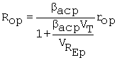
where Rop
is the signal resistance looking up into the collector of the pnp. For example,
if REp is selected to produce VREp = 1 V and bacp = 50, the denominator is roughly 2, such that
Rop ![]() bacp/2)rop.
In this case, the load on the amplifier is due almost entirely to the output
resistance looking into the collector of the npn (Ron = ron),
with the result that the gain is [from C.44
bacp/2)rop.
In this case, the load on the amplifier is due almost entirely to the output
resistance looking into the collector of the npn (Ron = ron),
with the result that the gain is [from C.44
Equation C.51
![]()
The other
extreme is for RBp >> rpp + REp, where Rop ![]() rop [(C.48 The gain
reverts to (C.42), repeated here
rop [(C.48 The gain
reverts to (C.42), repeated here
![]()
The npn - pnp amplifier circuit of Fig. C.10 is used in the project on the amplifier to investigate the signal-derived magnitude of the slope parameters of npn and pnp transistors. Using a bypass capacitor at the base of the npn, as discussed below, the signal circuit will effectively have RB = 0, and a gain measurement along with (C.51) yields VAFn. The gain will also be measured for the circuit without the capacitor and with RBp >> rpp + REp (by design). For this case, (C.42) applies and the gain measurement provides information on the combination output resistance parameter, VAFnp. Between the two measurements, values for both parameters are determined.
In the measurement circuit of the npn - pnp amplifier, the gain referred to the signal source (amplifier circuit gain) is
Equation C.52
![]()
where Ronp is the signal resistance at the output node (Fig. C.10), that is, the combined resistance looking back into the collects of the npn and pnp transistors. In general, this is
Equation C.53
![]()
With RBp
effectively made zero with the shunting capacitor, Ronp ![]() ron = VAFn/IC.
Without the capacitor, Rop is obtainable from (C.47) for use in (C.53
ron = VAFn/IC.
Without the capacitor, Rop is obtainable from (C.47) for use in (C.53
In the amplifier project, the circuit-gain equation (C.52) is used to convert measured gain into Ronp and then information on VAFn and VAFp. With the availability of these numbers, we can then calculate the gain produced by the transistor (base to collector), using (C.44
The circuit equations for the circuit of Fig. C.10 are (collector power supply through pnp base)
Equation C.54
![]()
and (npn base)
Equation C.55
![]()
In the
project on the amplifier, RBp is determined for a design collector
current. The selection uses (C.54) with, for example, VCC ![]() 9 V, that is, less than the maximum
available from the DAQ output. Then with RBn = RBp, VBBn
will be less than VCC by the amount of the drop across REp
(for example, 1 V). This makes the good assumption that bDCn
9 V, that is, less than the maximum
available from the DAQ output. Then with RBn = RBp, VBBn
will be less than VCC by the amount of the drop across REp
(for example, 1 V). This makes the good assumption that bDCn ![]() bDCp, A LabVIEW program then sets up the circuit
for the design collector current by adjusting two supply voltages (DAQ output
channels).
bDCp, A LabVIEW program then sets up the circuit
for the design collector current by adjusting two supply voltages (DAQ output
channels).
In the npn -
pnp amplifier project, we determine VAFn directly through a gain
measurement for a circuit configuration in which (C.51) is valid. The requirement that RBp
![]() 0 will be implemented by shunting the
base of the pnp transistor to ground with a capacitor, Cb, as shown
in Fig.
C.12.
The capacitor must be sufficiently large to hold the base at ground at the
frequency of the gain measurements.
0 will be implemented by shunting the
base of the pnp transistor to ground with a capacitor, Cb, as shown
in Fig.
C.12.
The capacitor must be sufficiently large to hold the base at ground at the
frequency of the gain measurements.
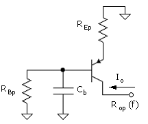
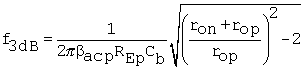
The expression to determine the required value of Cb can be obtained as follows: We start with the expression for Ro without Cb, which is (C.47) and repeated here (referring to the generalized circuit Fig. C.11
![]()
With the capacitor in parallel with RBp, RB in (C.47) is replaced with the impedance of the parallel combination of RBp and Cb. The resulting Rop is frequency dependent and is given by
Equation C.56
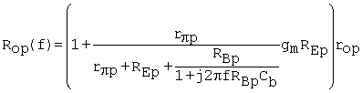
This can be manipulated into the form
Equation C.57
where
Equation C.58
![]()
and
Equation C.59
The
approximate form uses RBp >> rpp + REp. At f ![]() f1, Rop(f1)
f1, Rop(f1)
![]() rop, such that a good
approximation is obtained with dropping the "1" in the numerator. The approximate form is then
rop, such that a good
approximation is obtained with dropping the "1" in the numerator. The approximate form is then
Equation C.60
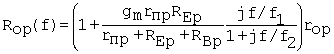
Further rearranging leads to
Equation C.61
![]()
where
Equation C.62
and
Equation C.63
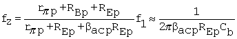
The approximate form again uses RBp >> rpp + REp.
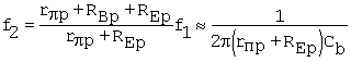
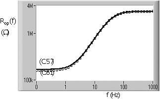
Mathcad-generated
plots of the magnitude of Rop(f) using (C.57) (and f2 and fz
exact) and (C.61) (with the approximate forms for f2
and fz) are shown in Fig.
C.13.
These are for VAFp = 150 V, bacp = 50, RBp = 330 KW, REp = 800 W, Cb = 2 mF and IC = 1 mA. Characteristic frequencies are fz
= 1.9 Hz and f2 = 38.2 Hz. The approximate form is very close to the
exact form except in the lowest frequency range. For f ![]() 0, Rop(f)
0, Rop(f) ![]() rop in both cases. For
example, in the exact and approximate cases, Rop(f) = 1.12rop
and Rop(f) = 1.05rop, respectively, for f = 0.
rop in both cases. For
example, in the exact and approximate cases, Rop(f) = 1.12rop
and Rop(f) = 1.05rop, respectively, for f = 0.
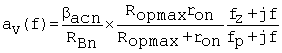
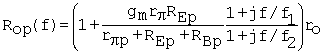
Substituting Rop(f) for Rop in (C.52), we obtain the frequency-dependent amplifier-circuit gain
Equation C.64
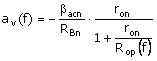
Then using (C.61) for Rop(f) in (C.64) results in
Equation C.65
![]()
where
Equation C.66
![]()
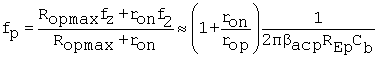
The approximate form uses Ropmax >> ron and the approximate f2 and fz.
The design
frequency f3dB is obtained from ![]() )]. Utilizing the approximate forms
of f2, fz, and fp, f3dB simplifies
to
)]. Utilizing the approximate forms
of f2, fz, and fp, f3dB simplifies
to
Equation C.67
The result is significantly lower than f2 in (C.61) because Rop(f) is in parallel with ron, which is much smaller than the high-frequency value of Rop(f). The parameter bacp appears from the association bacp = gmrpp C.15
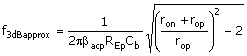
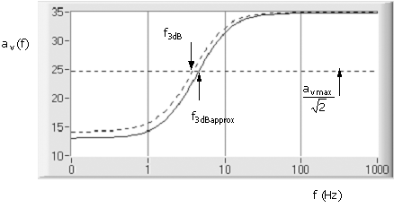
Mathcad-generated plots of (C.65) for the exact and approximate values for fp and fz are shown in Fig. C.14. The parameter and component values are from the plots of Fig. C.13 with the addition of VAFn = 250 V, bacn bacp = 50, and RBn = RBp = 330 kW. With capacitor Cb = 2 mF, f3dB = 3.8 H (exact fp and fz) and f3dBapprox = 4.5 Hz [(C.67
It was shown that the emitter resistor of the measurement circuit of Fig. C.10 can have a significant effect on output resistance. The emitter resistor has the effect of increasing the input resistance as well, such that it is compatible with high-resistance sources and the resistor adds to the bias stability. The common-emitter stage with an emitter resistor is, in fact, a very common configuration in BJT electronics.
Here, we analyze the effect of the emitter resistor on the input resistance (at the base) and on the gain of the common-emitter stage. The development leads directly to an assessment of the signal performance of the emitter-follower (common-collector) stage. The two aspects of the circuit with the emitter resistor are discussed in the following.
The
discussion is applicable to the circuit of Fig.
C.10,
where the input resistance is at the base of the pnp. In this circuit, RE![]() REp and, for the
analysis, a base signal voltage, Vb, is applied directly to the base
of the pnp. A general signal circuit for a common-emitter stage (output, Voce)
with emitter resistor is shown in Fig.
C.15.
Also indicated is the output for the emitter-follower stage (Voef).
REp and, for the
analysis, a base signal voltage, Vb, is applied directly to the base
of the pnp. A general signal circuit for a common-emitter stage (output, Voce)
with emitter resistor is shown in Fig.
C.15.
Also indicated is the output for the emitter-follower stage (Voef).
Assume that ro >> RL, such that we can neglect the current through ro. (This assumption is violated in the circuit of Fig. C.10, as the load is the output resistance of the npn, ron.) With this simplification, the loop equation at the input of the circuit is
Equation C.68
![]()
having used Vbe = Ibrp. The input resistance at the base is thus (with respect to signal ground)
Equation C.69
![]()
The following form of the result provides a convenient way of assessing the effect of the resistor on the input resistance:
Equation C.70
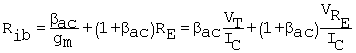
The result shows that with RE in the circuit, the input resistance is increased over that of the circuit without RE by a factor of approximately VRE/VT. For example, with VRE = 1 V, VRE/VT is about 40 at room temperature.
For the npn - pnp circuit of Fig. C.10, Rib at the base of the pnp is somewhat less than given by (C.70) because the effective load, that is, ron, is so large and the simplification made above, ro >> RL, is not valid. However, as is usually the case in design, such approximate forms are sufficient. This takes into consideration that exact solutions are not required or justified, given the variation in the model and circuit parameters that naturally occur.
If better
precision is, however, required, a good approximation for (C.70) is readily obtained by replacing,
in (C.70 bac with ![]() . This is specifically applied to
the circuit of Fig.
C.10,
where the input is at the base of the pnp and ron
. This is specifically applied to
the circuit of Fig.
C.10,
where the input is at the base of the pnp and ron![]() RL and the output
resistance of the pnp is rop. The approximation is based on the
expectation that Voce >> Voef Fig.
C.15
such that the voltages across ron and rop are similar.
RL and the output
resistance of the pnp is rop. The approximation is based on the
expectation that Voce >> Voef Fig.
C.15
such that the voltages across ron and rop are similar.
Equation C.71
![]()
Suppose that the gain expression is applied to the circuit of Fig. C.1(b) but with an emitter resistor installed. From the signal source, the gain is then
Equation C.72
![]()
where the resistance at the base, Rb, is now
Equation C.73
![]()
With (C.71) for the base-to-output gain,
Equation C.74
![]()
The result shows that the maximum gain is approximately RL/RE. Therefore, although the circuit can have good bias stability, the emitter resistor seriously reduces the signal gain. The circuit with a bypass capacitor would have a gain given by (C.19). The circuit with a bypass capacitor would still have the advantage of bias stability. Essentially all practical common-emitter circuits have the emitter resistor, with or without the bypass capacitor. A two-stage-circuit significant voltage gain without a capacitor is discussed in the next unit.
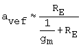
When the output is taken at the emitter instead of at the collector (Fig. C.15), the circuit becomes an emitter-follower amplifier stage. (The collector resistor is unnecessary and the collector terminal is connected to the power supply.) The output voltage in this case is
Equation C.75
![]()
The emitter-follower stage gain (transfer ratio) is the ratio of (C.75) and (C.68), that is
Equation C.76
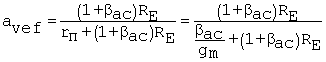
A magnitude assessment can be made from
Equation C.77
For example, with VRE = 1 V, avef = 0.97 at room temperature. The input resistance, from (C.70), for the same conditions in addition to IC = 0.1 mA and bac = 100 is Rib = 1 MW. The emitter-follower stage is seen to have a gain of approximately unity and a very high input resistance. Its primary role is therefore that of a buffer stage.
An alternative form for the emitter-follower stage gain is
Equation C.78
This is equivalent to a unity-gain amplifier with an output resistance of 1/gm. The output resistance is, for example, about 26 W at IC = 1 mA. Therefore, when an external load is attached to the emitter-follower stage output, the gain remains near unity for very small load values.
An example of an application that takes advantage of the characteristics of the emitter-follower stage is shown in Fig. C.16. This is a cascade of an emitter-follower stage and a common-emitter stage. The overall gain is the product of the input network function and the gains of the two stages. That is,
Equation C.79
![]()
where ![]() . For example, suppose that bac = 100 and that the bias collector currents are
IC1 = 0.1 mA and IC2 = 10IC1 = 1 mA. The
emitter resistor is RE = VBE/IC1 = 6000W (neglecting the base current, IB2) with VBE = 0.6
V such that
. For example, suppose that bac = 100 and that the bias collector currents are
IC1 = 0.1 mA and IC2 = 10IC1 = 1 mA. The
emitter resistor is RE = VBE/IC1 = 6000W (neglecting the base current, IB2) with VBE = 0.6
V such that ![]() and the gain of the emitter-follower
stage is 0.87. With VCC = 10 V and VCE = 5 V, the gain of
the common-emitter stage is -192. Both gains are at room temperature.
Therefore, the gain from the base of the emitter-follower stage to the output
is -168.
and the gain of the emitter-follower
stage is 0.87. With VCC = 10 V and VCE = 5 V, the gain of
the common-emitter stage is -192. Both gains are at room temperature.
Therefore, the gain from the base of the emitter-follower stage to the output
is -168.
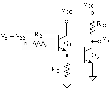
The input
resistance at the base of the emitter follower is Rib ![]() 500 kW. Assume, for example, that RB
500 kW. Assume, for example, that RB ![]() 50 kW. The overall gain for this case is -136. By comparison, the circuit,
which omits the emitter-follower stage (RB connected directly to the
base of the common-emitter stage), has a gain of -9.5.
50 kW. The overall gain for this case is -136. By comparison, the circuit,
which omits the emitter-follower stage (RB connected directly to the
base of the common-emitter stage), has a gain of -9.5.
|
|
Transconductance. |
|
|
Emitter-base junction common-emitter stage input resistance. |
|
|
Collector - emitter output resistance. |
|
|
Total base - emitter input resistance. |
|
|
Base current equation for common-emitter amplifier. |
|
|
Collector current equation for common-emitter amplifier. |
|
|
Collector power-supply voltage solution common-emitter amplifier with single power supply. |
|
|
Base-to-collector gain. Neglect internal output resistance of driver transistor. |
|
|
Overall gain from function generator (signal source). |
|
|
Overall gain with very large source resistor, Rs, as in amplifier gain experiments. Rs >> rp, RB >> rp |
|
|
Base-to-collector gain expression that includes the output resistance of the transistor. |
|
|
Base-to-collector
large-signal "gain" that includes nonlinearity of IC, VBE
relationship. Linear relation applies when Ic/IC ratio
is small enough for ln(1 + Ic/IC) |
|
|
General solution for base-to-collector gain for npn - pnp amplifier with emitter resistor, REp. |
|
|
Output resistance at collector with emitter resistor (general). |
|
|
Base-to-collector gain of npn - pnp amplifier, REp = 0. |
|
|
Approximate base-to-collector gain of npn - pnp amplifier with emitter resistor REp (and RBp = 0). |
|
|
Frequency-dependent output resistance at the collector of pnp with REp |
|
|
Characteristic frequencies of Rop(f) function. |
|
|
Frequency-dependent amplifier gain of npn - pnp amplifier with emitter resistor and base-bypass capacitor. |
|
|
Characteristic frequency of av(f) function. |
|
|
Maximum output resistance at the collector of the pnp with emitter resistor. |
|
|
Design equation for selecting Cb for npn - pnp measurement circuit. |
|
|
Input resistance at base of common-emitter stage with emitter resistor. |
|
|
Gain of the emitter-follower stage. |
|
|
Alternative form of the gain of the emitter-follower stage. |
|
Project Mathcad Files |
ExerciseC1.mcd - ProjectC1.mcd - ExerciseC2 - ProjectC2.mcd |
|
Laboratory Project C1 |
NPN Common-Emitter Amplifier |
|
PC.2 |
DC Circuit Setup and Parameter Determination |
|
PC.3 |
Amplifier Gain at One Bias Current |
|
PC.4 |
Amplifier Gain versus Bias Current |
|
PC.5 |
Gain-Measurement Frequency Response |
|
Laboratory Project C2 |
NPN - PNP Common-Emitter Amplifier with Current-Source Load |
|
PC.7 |
Measurement of the PNP Parameters |
|
PC.8 |
DC Circuit Setup |
|
PC.9 |
Measurement of the Amplifier Gain |
|