In this unit, we present a basic review of segments of circuit analysis which recur repeatedly in electronic circuits. A firm grasp on these is essential to developing an understanding of the analysis and design of basic electronic circuits. A transistor is included in the circuits to show a correlation between circuit analysis and electronics. Only steady-state circuit situations are considered here. This includes dc and sinusoidal. Some transient analysis is considered in connection with operational amplifier applications with capacitors.
Figure 1.1(a) shows a basic NMOS amplifier stage. This is the dc (or bias) portion of the circuit, which excludes the signal part. The terminals of the transistor are designed G (gate), D (drain) and S (source). The design calls for a dc voltage VG, with respect to the zero reference voltage, which is obtained by dividing the supply voltage VDD between bias resistors RG1 and RG2. Since the gate terminal has zero current, the voltage, VG, at the gate can be assessed with the resistor network separated from the circuit as in Fig. 1.1(b). The goal is to relate the node voltage VG to the values of RG1 and RG2 and VDD. The result is the basic resistor voltage-divider relation.
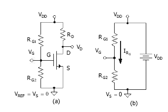
Note that since VDD is given with respect to the reference zero volts, the VDD designation at the top node is equivalent to the supply voltage, also referred to as VDD. The current IRG is
Equation 1.1
The voltage across the resistor RG2 is VG (since VG is with respect to the zero reference) and this is
Equation 1.2
It can be concluded that the gate voltage is the value of RG2 divided by the sum of the two gate-bias resistors.
For the dc circuit in Fig. 1.1, the drain voltage is determined from
Equation 1.3
![]()
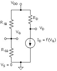
As illustrated in Fig. 1.2, for the purpose of a solution to ( ), the transistor can be replaced by a current source as shown in Fig. 1.2. Drain current ID is a function of VG; that is, ID = f(VG). Thus, in a design, the value of VG determines the value of VD. ID is related to VG according to
Equation 1.4
![]()
This relation and parameters Vtno and kn are discussed in Unit 2
Capacitance
associated with amplifiers may cause the output to fall off at low and high
frequencies. This effect is referred to as the frequency
response of the amplifier. A generalization of possible capacitance is
shown in the circuit of Fig.
1.3.
Capacitor Cg is an external capacitance, which is included to attach
a sine-wave signal source, consisting of Vsig (e.g., sine-wave peak)
and Rs, without interrupting the dc bias circuitry. Similarly, there
could be an output capacitance, which couples the signal output voltage to an
external load resistor.
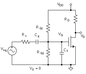
Generally, the frequency range over which a given capacitor is effective is much different for the two capacitors. Capacitor Cg affects the output at low frequencies, while the effect of CT is realized at the high end of the spectrum. Thus, their effects can be considered separately if, as assumed in the following, the high and low ends of the response function are widely separated in frequency, that is, by several orders of magnitude.
Figure 1.4 shows the signal circuits for the two cases of low (a) and high (b) frequencies. As discussed in Unit 2, the signal circuit is formulated from the complete circuit by setting all dc voltages to zero. This includes, for this amplifier, the power supply and dc voltage across the capacitor Cg. Note that the transistor plays no apparent role in the frequency response in the equivalent circuit. It is, of course, critically important in dictating the value of CT.
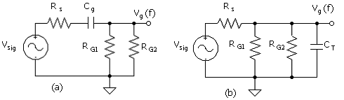
The two circuits, (a) and (b), are technically high-pass and low-pass circuits, respectively. In combination, they have a midband range, which is the normal range of frequency for operation of the amplifier. As mentioned above, if the midband separates the low and high portions by a sufficient range of frequency, the effects may be considered separately, as suggested in Fig. 1.4
The response function is obtained by considering the frequency dependence of the node voltage Vg(f) for the constant-magnitude sine-wave source voltage, Vsig. (Since the only voltages under consideration in the circuits of Fig. 1.4 are those associated with signals, lowercase subscript is used. This is discussed further in Unit 2
The frequency response is first considered for the low end of the spectrum and involves Cg only, as in the circuit of Fig. 1.4(a). We can utilize the voltage-divider relation obtained above as ( For this case this is
Equation 1.5
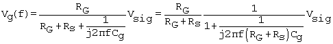
where RG = RG1 || RG2.
Using the definitions
Equation 1.6
![]()
and
Equation 1.7
![]()
the result is condensable to
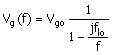
Equation 1.8
The magnitude is
Equation 1.9
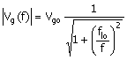
At f = flo, ![]() . This, by definition, is the
response magnitude for the 3-dB frequency, f3dB, for the
low-frequency end of the response function. That is, in general, f3dB
is the frequency at which the response falls to
. This, by definition, is the
response magnitude for the 3-dB frequency, f3dB, for the
low-frequency end of the response function. That is, in general, f3dB
is the frequency at which the response falls to ![]() (for decreasing frequency) from the
maximum, asymptotic value. Thus, for the simple case here of one capacitor, f3dB
= flo.
(for decreasing frequency) from the
maximum, asymptotic value. Thus, for the simple case here of one capacitor, f3dB
= flo.
The equation for the response function associated with CT is similar to ( ) and is
Equation 1.10
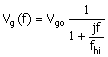
where
Equation 1.11
![]()
The frequency f3dB for this case is just fhi. The frequency response of circuits of the type of Fig. 1.4 is measured in Project 1. In the design of the project circuits, capacitors and resistors are selected to give widely different flo and fhi values.
|
|
Resistor-circuit voltage divider. |
|
|
Drain current and gate voltage relation. |
|
|
Low-frequency frequency-response function. |
|
|
High-frequency frequency-response function. |
|
|
Midband magnitude of the signal gate voltage. |
|
Project Mathcad Files |
Exercise01.mcd - Project01.mcd |
|
Laboratory Project 1 |
Basic Circuit Analysis for Electronic Circuits and Programming Exercises |
|
P1.1 |
Resistor Voltage-Divider Measurements |
|
P1.2 |
Resistor Voltage Divider with Current Measurement |
|
P1.3 |
Resistor Voltage Divider with Resistor Measurement |
|
P1.4 |
Resistor Voltage Divider with a Sine-Wave Source Voltage |
|
P1.5 |
Frequency Response of a Resistor-Capacitor Circuit |
|
