|
|
|
Hardware Engineering Specification
Model:
![]()

Mitac Confidential
Rev: 02
|
Hardware Design Division, Mitac Technology Corp. |
Aug, 6,2002 |
Reverse history
|
R.00 |
8500 draft H/W engineer spec.(12/18/2001) Andy.shih |
|
R.01 |
8500 EVT2 H/W engineer spec. (3/27/2002) Andy.shih |
|
R.02 |
8500 MP H/W engineer spec. (8/6/2002) Zan-Yi Chang |
|
R.03 | |
|
R.04 | |
|
R05 |
The information contained in this
document is subject to change without notice. Mitac Technology Corp.
makes no warranties, either express or implied, in this document. The
entire risk of the use or the results of the use of this document remains
with the user. No part of this document may be reproduced or transmitted
in any form or by any means, electronic or mechanical, for any purpose,
without the express written permission of Mitac Technology Corp.. Please try to use
recycled paper. Copyright Mitac Technology Corp.. All rights reserved.
The 8500 motherboard would support the Intel® Pentium® 4 processor with FCPGA packaged, mPGA 478 Socket, which will supports the different levels up to Willamette P4 1.7GHz (Throttling) / Northwood above 2.0 GHz(Throttling)
This
system is based on PCI architecture, which have standard hardware peripheral
interface. The power management complies with Advanced Configuration and Power
Interface (ACPI) 1.0. It also provides easy configuration through CMOS setup,
which is built in system BIOS software and can be pop-up by pressing F2 at
system start up or warm reset. System also provides ico LEDs to display system
status, such as Power indicator,
The memory subsystem supports 0MB on board memory,Two JEDEC-standard 200-pin, small-outline, dual in-line memory module (SODIMM) ,Support PC2100 & PC2700.
SiS650 IGUI Host Memory Controller integrates a high performance host interface for Intel Pentium 4 processor, a high performance 2D/3D Graphic Engine, a high performance memory controller, an AGP 4X interface, and SiS MuTIOL® Technology connecting w/ SiS961 MuTIOL® Media IO.
The SiS961 MuTIOL® Media I/O integrates the Audio Controller with AC 97 Interface, the Ethernet MAC, the Dual Universal Serial Bus Host Controllers, the IDE Master/Slave controllers, and the MuTIOL® Connect to PCI bridge. The PCI to LPC bridge, I/O Advanced Programmable Interrupt Controller, legacy system I/O, I/O Advanced Programmable Interrupt Controller and legacy power management functionalities are also integrated. The SiS961 also incorporates an universal interface supporting the asynchronous inputs/outputs of the X86 compatible microprocessors like PIII, K7, and P4.
The CH7017 is a Display Controller device which accepts two digital graphics input data streams. One data stream outputs through an LVDS transmitter to an LCD panel, while the other data stream is encoded for NTSC or PALTV and outputs through a 10-bit high speed DAC. The TV encoder device encodes a graphics signal up to 1024x768 resolution and outputs the video signals according to NTSC or PAL standards. The LVDS transmitter operates at pixel speeds up to 165MHz per link, supporting 1600x1200 panels at 60Hz refresh rate.
To provide for the increasing number of multimedia applications, the AC97 CODEC ALC201 is integrated onto the motherboard
A full set of software drivers and utilities are available to allow advanced operating systems such as Windows Me and Windows 2000 to take full advantage of the hardware capabilities such as bus mastering IDE, Windows 95-ready Plug & Play, Advanced Power Management (APM) and Advance configuration and power interface (ACPI).
Following chapters will have more detail description for each individual sub-systems and functions.
|
CPU |
Intel Desktop Pentium 4 Processors with OLGA Package, uFC-PGA 478 Socket Support upto P4 2.4GHz (Target Thermal ceiling 65W) |
|
Core logic |
SiS 650+SiS961: Host & Memory & AGP Controller integrates a high performance host interface for Intel Pentium 4 processor, a high performance memory controller, a AGP interface, and SiS MuTIOL® ® Technology connecting w/ SiS961 MuTIOL® Media IO. |
|
VGA Control |
Chrontel CH7017 |
|
System BIOS |
256KB Flash EPROM Inside -Includes System BIOS, VGA BIOS, and plug & Play capability, ACPI |
|
Memory |
0MB on board memory -Two JEDEC-standard 200-pin, small-outline, dual in-line memory module (SODIMM) -Support PC2100 & PC2700 |
|
Video Memory |
8/16/32/64 UMA |
|
Clock Generator DDR Clock Buffer |
ICS 952001 ICS 93722 |
|
IEEE1394 |
MB86613S |
|
Audio System |
AC97 CODEC: Advance Logic, Inc, ALC201 Power Amplifier: TI TPA0202 |
|
Super I/O |
W83697HG |
|
Modem |
56Kbps(V.90, worldwide) MDC Modem |
|
PHY of LAN |
ICS1893Y-10 10/100 base T PHY |
The Intel® Pentium® 4 processor, Intel's most advanced, most powerful processor, is based on the new Intel® NetBur 16116l1122q stT micro-architecture. The Pentium 4 processor is designed to deliver performance across applications and usages where end users can truly appreciate and experience the performance. These applications include Internet audio and streaming video, image processing, video content creation, speech, 3D, CAD, games, multi-media, and multi-tasking user environments. The Intel Pentium 4 processor delivers this world-class performance for consumer enthusiast and business professional desktop users as well as for entry-level workstation users.
Highlights of the Pentium 4 processor:
Available at speeds ranging from 1.50 to 2 GHz
Featuring the new Intel NetBurst micro-architecture
Supported by the SiS 650 chipset
Fully compatible with existing Intel Architecture-based software
Internet Streaming SIMD Extensions 2
Intel® MMXT media enhancement technology
Memory cacheability up to 4 GB of addressable memory space and system memory scalability up to 64GB of physical memory
Support for uni-processor designs
Based upon Intel's 0.18 micron manufacturing process
![]()
INTEL PENTIUM 4 PROCESSOR PRODUCT FEATURE HIGHLIGHTS
The Intel NetBurst micro-architecture delivers a number of new and innovative features including Hyper Pipelined Technology, 400 MHz System Bus, Execution Trace Cache, and Rapid Execution Engine as well as a number of enhanced features Advanced Transfer Cache, Advanced Dynamic Execution, Enhanced Floating-point and Multi-media Unit, and Streaming SIMD Extensions 2. Many of these new innovations and advances were made possible with improvements in processor technology, process technology, and circuit design that could not previously be implemented in high-volume, manufacturable solutions. The features and resulting benefits of the new micro-architecture are defined below.
o Non-Blocking, full speed, on-die Level 2 cache
o 8-way set associativity
o 256-bit data bus to the level 2 cache
o Data clocked into and out of the cache every clock cycle
Programmable Timing Control HubT for P4T processor
General Description
The ICS952001 is a two chip clock solution for desktop designs using SIS 645/650 style chipsets. When used with a zero delay buffer such as the ICS9179-06 for PC133 or the ICS93705 for DDR applications it provides all the necessary clocks signals for such a system.
The ICS952001 is part of a whole new line of ICS clock generators and buffers called TCHT (Timing Control Hub). ICS is the first to introduce a whole product line which offers full programmability and flexibility on a single clock device. Employing the use of a serially programmable I2C interface, this device can adjust the output clocks by configuring the frequency setting, the output divider ratios, selecting the ideal spread percentage, the output skew, the output strength, and enabling/disabling each individual output clock. TCH also incorporates ICS's Watchdog Timer technology and a reset feature to provide a safe setting under unstable system conditions. M/N control can configure output frequency with resolution up to 0.1MHz increment.
Recommended Application:
SIS 645/650 style chipsets.
Output Features:
2 - Pairs of differential CPUCLKs @ 3.3V.
1 - SDRAM @ 3.3V
8 - PCI @3.3V
2 - AGP @ 3.3V
2 - ZCLKs @ 3.3V
1 - 48MHz, @3.3V fixed
1 - 24/48MHz, @3.3V selectable by I2C
3 - REF @3.3V, 14.318MHz.
Features/Benefits
Programmable output frequency, divider ratios, output rise/fall time, output skew.
Programmable spread percentage for EMI control.
Watchdog timer technology to reset system if system malfunctions
Programmable watch dog safe frequency.
Support I2C Index read/write and block read/write operations
For PC133 SDRAM system use the ICS9179-06 as the memory buffer.
For DDR SDRAM system use the ICS93705 as the memory buffer.
Uses external 14.318MHz crystal.
Key Specifications:
PCI - PCI output skew: < 500ps
CPU - SDRAM output skew: < 1ns
AGP - AGP output skew: <150ps
Low Cost DDR Phase Lock Loop Zero Delay Buffer
Recommended Application:
SIS 645/650 style chipsets.
Product Description/Features:
Low skew, low jitter PLL clock driver
I2C for functional and output control
Feedback pins for input to output synchronization
Spread Spectrum tolerant inputs
3.3V toerant CLK_INT input
Switching Characteristics:
PEAK - PEAK jitter (66MHz): <120ps
PEAK - PEAK jitter (>100MHz): <75ps
CYCLE - CYCLE jitter (66MHz):<120ps
CYCLE - CYCLE jitter (>100MHz):<65ps
OUTPUT - OUTPUT skew: <100ps
Output Rise and Fall Time: 650ps - 950ps
DUTY CYCLE: 49.5% - 50.5%
SiS650 IGUI Host Memory Controller integrates a high
performance host interface for Intel Pentium 4 processor, a high performance
2D/3D Graphic Engine, a high performance memory controller, an AGP 4X
interface, and SiS MuTIOL® Technology connecting w/ SiS961 MuTIOL® Media IO.
SiS650 Host Interface features the AGTL
& AGTL+ compliant bus driver technology with integrated on-die
termination to support Intel Pentium 4 processors. SiS650 provides a 12-level
In-Order-Queue to support maximum outstanding transactions up to 12. It
integrated a high performance 2D/3D Graphic Engine, Video Accelerator and
Advanced Hardware Acceleration MPEGI/MPEGII Video Decoder for the Intel Pentium
4 series based PC systems. It also integrates a high performance 2.1GB/s DDR266
Memory controller to sustain the bandwidth demand from the integrated GUI or
external AGP master, host processor, as well as the multi I/O masters. In
addition to integrated GUI, SiS650 also can support external AGP slot with AGP
1X/2X/4X capability and Fast Write Transactions. A high bandwidth and mature
SiS MuTIOL® technology is incorporated to connect SiS650 and SiS961 MuTIOL®
Media I/O together. SiS MuTIOL® technology is developed into three layers, the
Multi-threaded I/O Link Layer delivering 1.2GB bandwidth to connect embedded
DMA Master devices and external PCI masters to interface to Multi-threaded I/O
Link layer, the Multi-threaded I/O Link Encoder/Decoder in SiS961 to transfer
data w/ 533 MB/s bandwidth from/to Multi-threaded I/O Link layer to/from
SiS650, and the Multi-threaded I/O Link Encoder/Decoder in SiS650 to transfer
data w/ 533 MB/s from/to Multi-threaded I/O Link layer to/from SiS961.
An Unified Memory Controller supporting
PC133 or DDR266 DRAM is incorporated, delivering a high performance data
transfer to/from memory subsystem from/to the Host processor, the integrated
graphic engine or external AGP master, or the I/O bus masters. The memory
controller also supports the Suspend to RAM function by retaining the CKE# pins
asserted in ACPI S3 state in which only AUX source deliver power. The SiS650
adopts the Shared Memory Architecture, eliminating the need and thus the cost
of the frame buffer memory by organizing the frame buffer in the system memory.
The frame buffer size can be allocated from 8MB to 64MB.
The Integrated GUI features a high
performance 3D accelerator with 2 Pixel / 4 Texture, and a 128 bit 2D
accelerator with 1T pipeline BITBLT engine. It also features a Video
Accelerator and advanced hardware acceleration logic to deliver high quality
DVD playback. A Dual 12 bit DDR digital video link interfaced to SiS 301B
Two separate buses, Host-t-GUI in the
width of 64 bit, and GUI-t-Memory Controller in the width of 128 bit are
devised to ensure concurrency of Host-t-GUI streaming, and GUI-t-MC streaming.
In PC133, or DDR266 memory subsystem, the 128 bit GUI-t-MC bus will attain the
AGP4X or AGP 8X equivalent texture transfer rate, respectively. The Memory
Controller mainly comprises the Memory Arbiter, the M-data/M-Command Queues,
and the Memory Interface. The Memory Arbiter arbitrates a plenty of memory
access requests from the GUI or AGP controller, Host Controller, and I/O bus
masters based on a default optimized priority list with the capability of
dynamically prioritizing the I/O bus master requests in a bid to offering
privileged service to 1) the isochronous downstream transfer to guarantee the
min. latency & timely delivery, or 2) the PCI master upstream transfer to
curb the latency within the maximum tolerant period of 10us. Prior to the
memory access requests pushed into the M-data queue, any command compliant to
the paging mechanism is generated and pushed into the M-CMD queue. The
M-data/M-CMD Queues further orders and forwards these queuing requests to the
Memory Interface in an effort to utilizing the memory bandwidth to its utmost
by scheduling the command requests in the background when the data requests
streamlines in the foreground.
The SiS961 MuTIOL®
Media I/O integrates the Audio Controller with AC 97 Interface, the
Ethernet MAC, the Dual Universal Serial Bus Host Controllers, the IDE
Master/Slave controllers, and the MuTIOL® Connect to PCI bridge. The PCI to LPC
bridge, I/O Advanced Programmable Interrupt Controller, legacy system I/O, I/O
Advanced Programmable Interrupt Controller and legacy power management
functionalities are also integrated. The SiS961 also incorporates an universal
interface supporting the asynchronous inputs/outputs of the X86 compatible
microprocessors like PIII, K7, and P4.
The Integrated Audio Controller
features a 6 channels of AC 97 v2.2 compliance audio to present 5.1-channel
Dolby digital material or to generate stereo audio with simultaneous V.90 HSP
modem operation. Besides, 4 separate SDATAIN pins are provided to support
multiple audio Codecs + one modem Codec maximally, effectuating the realization
of 5.1 channel Dolby digital material in theater quality sound. Both
traditional consumer digital audio channel as well as the AC 97 v2.2 compliant
consumer digital audio slot are supported. VRA mode is also associated with
both the AC 97 audio link and the traditional consumer digital audio channel.
The integrated Fast Ethernet MAC
features an IEEE 802.3 and IEEE 802.3x compliant MAC supporting full duplex 10
Base-T, 100 Base-T Ethernet, or 1Mb/s & 10Mb/s Home networking. 5 wake-up
Frames, Magic Packet and link status change wake-up functions in G1/G2 states
are supported. Besides, the integrated MAC provides a scheme to store the MAC
address without the need of an external EEPROM. The 25 MHz oscillating circuit
is integrated so as only an external low cost 25 MHz crystal is needed for the
clocking system.
The integrated Universal Serial Bus Host
Controllers features Dual Independent OHCI Compliant Host controllers with
six USB ports delivering 2 x 12 Mb/s bandwidth and rich connectivity. Besides,
each port can be optionally configured as the wake-up source. Legacy USB
devices as well as over current detection are also implemented. The integrated
IDE Master/Slave controllers features Dual Independent IDE channels supporting
PIO mode 0,1,2,3,4, and Ultra DMA 33/66/100. It provides two separate data
paths for the dual IDE channels that sustain the high data transfer rate in the
multitasking environment. The MuTIOL® Connect to PCI bridge supporting 6 PCI master
is compliant to PCI 2.2 specification. The SiS961 also incorporates the legacy
system I/O like: two 8237A compatible DMA controllers, three 8254 compatible
programmable 16-bit counters, hardwired keyboard controller and PS2 mouse
interface, Real Time clock with 256B CMOS SRAM and two 8259A compatible
Interrupt controllers. Besides, the I/O APIC managing up to 24 interrupts with
both Serial and FSB interrupt delivery modes is supported.
The integrated power management module
incorporates the ACPI 1.0b compliance functions, the APM 1.2 compliance
functions, and the PCI bus power management interface spec. v1.1. Numerous
power-up events and power down events are also supported. 21 general purposed
I/O pins are provided to give an easy to use logic for specific application. In
addition, the SiS961 supports Intel Speed Step technology and Deeper Sleep
power state for Intel Mobile processor. For AMD processor, the SiS961 use the
CPUSTP# signal to reduce processor voltage during C3 and S1 state.
SiS301LV, which is an accompany chip of SiS VGA chip, integrates
A NTSC/PAL video encoder with Macrovision Ver.7.1.L1 option for TV display.
A LVDS transmitter with bi-linear scaling capability for TFT LCD panel display.

All the above functions can support dual-display features. It means that the
second display device driven by SiS301LV can display independent resolutions,
color depths and frame rates different from the traditional CRT monitor driven
by primary VGA chip. SiS301LV receives digital video signals and control
signals from the primary VGA chip then transforms them into composite, S or
component video output for TV display, LVDS signals for LCD display. The output display combination can be one of
the three : (1) Primary CRT+SiS301LV TV, (2) Primary CRT+SiS301LV LCD,(3)
SiS301LV TV + SiS301LV LCD.
Supports PAL and NTSC Systems.
Supports Composite, S-Video, and Component RGB( SCART) Output Signals
Supports Macrovision Copy Protection Process Rev. 7.1.L1
Support Progressive TV 525P YPbPr Output Signals.
Support Macrovision Conpy Protection Waveforms for 525p Progressive Scan Output
Supports TV/Primary VGA Independent Display Resolution and Frame Rate at Enhanced Mode
Provides Adaptive 6-Line Anti-Flicker Filtering.
Provides Hardware Interpolation for Programmable Under-Scan/Over-Scan Adjustment.
Provides Programmable Display Position Adjustment.
Provides Programmable Notch Filter for Cross Color Elimination.
Provides Chrominance Filter for Cross Luminance Elimination
Provides Color Saturation Adjustment for Vivid TV Output.
Provides Gamma Correction Independent of That of Primary VGA.
Auto-Sense of TV Connection
Supports LVDS Transmitter Function.
Single LVDS supports pixel rate up to 110M pixel/sec.
Compatible with TIA/EIA-644 LVDS standard.
Provides Bi-Linear Scaling to Scale VGA Low Resolution Mode up for LCD Display-up to 1280x1024.
Supports LCD/Primary VGA Independent Display Resolution and Frame Rate at Enhanced Mode.
Support 2D dither for 18-bit panels.
Provides Programmable Display Centering.
Compliant with VESA DDC2B
Compliant with VESA Plug & Display, Hot Plugging Function.
SiS 961 is an AC'97 2.1 compliant controller that communicates with companion Codecs SiS a digital serial link called the AC-link.
The ALC201 is an AC97 2.2 compatible stereo audio codec designed for PC multimedia systems.The ALC201 prives the way for PC98 and PC99-compliant desktop, portable, and entertainment PCs, where high-quality audio is required.
The ALC201 AC'97 CODEC provides a complete high quality audio solution.
Features
l Single chip audio CODEC with high S/N ratio (>90 dB).
l 18-bit ADC and DAC resolution.
l Compliant with AC'97 2.2 specification
l Meet performance requirements for audio on PC2001 systems
l 18-bit stereo full-duplex CODEC with independent and variable sampling rate.
l 4 analog line-level stereo input with 5-bit volume control: LINE_IN, CD, VIDEO, AUX
l 2 analog line-level mono input: PC_BEEP, PHONE_IN.
l Mono output with 5-bit volume control.
l Stereo output with 5-bit volume control.
l 2 MIC inputs: Software selectable.
l Power management.
l 3D Stereo Enhancement
l Headphone output with 50mW/20ohm driving capability (ALC201
l Line output with 50mW/20ohm driving capability (ALC201A
l Headphone jack-detect function to mute LINE output.
l Multiple CODEC extension.
l MC 97 chained in allowed for multi-channel application.
l External Amplifier power down capability.
l Support S/PDIF out is fully compliant with AC 97 specification rev2.2
l DC offset cancellation.
l Power support: Digital: 3.3V Analog: 5V
l Standard 48-Pin LQFP Package
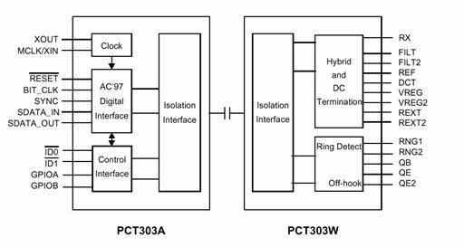
The PCT2303W chipset is designed to meet the demand of this emerging worldwide AMR/MDC market. The combination of PC-TEL's well proven PCT2303W chipset and the HSP56TM MR software modem driver allows systems manufactures to implement modem functions in PCs at a lower bill of materials (BOM) while maintaining higher system performance.
PC-TEL has streamlined the traditional modem into the Host Signal Processing (HSP) solution. Operating with the Pentium class processors, HSP becomes part of the host computer's system software. It requires less power to operate and less physical space than standard modem solutions. PC-TEL's HSP modem is an easily integrated, cost-effective communications solution that is flexible enough to carry you into the future.
The PCT2303W chip set is an integrated direct access arrangement (DAA) and Codec that provides a programmable line interface to meet international telephone line requirements. The PCT2303W chip set is available in two 16-pin small outline packages (AC'97 interface on PCT303A and phone-line interface on PCT303W). The chip set eliminates the need for an AFE, an isolation transformer, relays, opto-isolators, and 2-to 4-wire hybrid. The PCT2303W chip set dramatically reduces the number of discrete components and cost required to achieve compliance with international regulatory requirements. The PCT2303W complies with AC'97 Interface specification Rev. 2.1.
The chip set is fully programmable to meet worldwide telephone line interface requirements including those described by CTR21, NET4, JATE, FCC, and various country-specific PTT specifications. The programmable parameters of the PCT2303W chip set include AC termination, DC termination, ringer impedance, and ringer threshold. The PCT2303W chip set has been designed to meet stringent worldwide requirements for out-of-band energy, billing-tone immunity, lightning surges, and safety requirements.
tOperating System Compatibility
Windows 98 / NT4.0 /Win 2K /Win XP
tCompatibility
ITU-T V.90 56000,54667,53333,52000,50667,49333,48000,46667,45333,
42667,41333,40000,38667,37333,36000,34667,33333,32000,
30667,29333, 28000bps
K56Flex 56000,54000,52000,50000,48000,46000,44000,42000,40000,
38000,36000, 32000bps.
ITU-T V.34Annex 33600,31200 bps.
ITU-T V.34 28800 bps
ITU-T V.32bis 14400 bps
ITU-T V.32 9600,4800 bps
ITU-T V.22bis 2400 bps
ITU-T V.22 1200 bps
ITU-T V.21 300 bps
ITU-T V.23 1200/75 bps
ITU-T V.17 14400,12000,9600,7200 bps
ITU-T V.29 9600,7200 bps
ITU-T V.27ter 4800,2400 bps
tModulation
56000bps(V90&K56Flex) PCM
33600 bps (V.34Annex) TCM
28800 bps (V.34) TCM
14400 bps (V.32bis) TCM
12000 bps (V.32bis) TCM
9600 bps (V.32bis) TCM
7200 bps (V.32bis) QAM
9600 bps (V.32) TCM, QAM
4800 bps (V.32) QAM
14400 bps (V.17) TCM
12000 bps (V.17) TCM
9600 bps (V.29) QAM
7200 bps (V.29) QAM
4800 bps (V.27ter) DPSK
2400 bps (V.27ter) DPSK
2400 bps (V.22bis) QAM
1200/75bps (V.23) FSK
1200bps(V.22/Bell 212A) DPSK
300bps(V.21/Bell 103) FSK
tData Compression
V.42bis, MNP5
tError Correction
V.42 LAPM, MNP 2-4
tDTE interface
tDTMF Tone Frequency
Low Group Frequency (Hz)
|
697 |
770 |
852 |
941 |
||
|
High Group |
1 |
4 |
7 |
* |
|
|
Frequency |
2 |
5 |
8 |
0 |
|
|
(Hz) |
3 |
6 |
9 |
# |
|
|
A |
B |
C |
D |
tDTMF signal level
tDialing Type
Tone or pulse dialing
tTelephone Line interface
RJ-11
tReturn Loss
300HZ - 3400HZ >= 10db
tFlow Control
XOFF/XON or RTS/CTS
tReceive Level
-35 +/- 2dBm
tTransmit Level
>-15 dBm
Specification and features subject to change without notice!
2.6 MDC: PCTel MODEM DAUGHTER CARD PCT2303W
2.7.1 Overview
MB86613S is Fujitsu's IEEE1394- OHCI (Open Host Controller Interface) Controller LSI that is compliant with
IEEE1394- 1995, P1394a and OHCI (revision 1.1, release) standard drafts. This LSI integrates both 1394
PHY and LINK layers including analog PLL, transceiver, and comparator circuits using Fujitsu's advanced full
CMOS process for the cost- effective single- chip solution.
In addition to the 1394 block, the MB86613S contains various DMA engines called ContextProgram Controllers
used for OHCI functions and PCI block. ContextProgram block consists of total 13 channels of independent
DMA that are each dedicated to asynchronous and isochronous transmit and isochronous- asynchronous
common receive operations. On- chip, 5V and 3.3V operable, PCI bus controller is compliant with PCI
local bus standard (revision2.2) incorporating one 32- bit DMA controller and power management functions
as specified in PCI bus power management specification (version 1.1).
For valuable host side design, this chip also incorporates serial Configuration ROM interface.
The device operates by +5V or +3.3V power supply for the PCI andDMA blocks and +3.3V for the whole 1394
block.
To provide with the cost- effective solution, the LSI is housed in a 100- pin plastic small QFP package.
2.7.2. Features
1) 1394 Serial Bus Controller Block:
t Compliant with IEEE1394- 1995 and P1394a draft2.0
t Integrates PHY and LINK layers into single- chip.
t 1394 port number : 1 port
t Transfer Data Rate : S100, S200, and S400
t On- chip PLL : 400MHz for PHY and 50MHz for Link core.
t Cycle- Master Function
t On- chip Bus Management CSRs
t 6- pin cable supported
t On- chip transceiver and comparator
t On- chip another comparator for detecting the cable power
2) ContextProgram Controller Block :
t Compliant with Open HCI standard draft (revision 1.1)
t Total 13 independent ContextProgram Controllers:
a) Asynchronous Transmit DMA : 2 channels for response and request each
b) Isochronous Transmit DMA : 4 channels
c) Receive DMA : 7 channels for Asynchronous response and request each, 4 isochronous,
and 1 self- ID receive
Preliminary
t On- chip 6KB FIFO :
a) Asynchronous T ransmit- FIFO : 1.5KB
b) Isochronous Transmit- FIFO : 1.5KB
c) Asynchronous/Isochronous Receive- FIFO : 3.0KB
t On- chip context program work memory : 128B x 3
3) PCI Bus Controller Block :
t Compliant with PCI local bus specification (revision 2.2)
t On- chip 32- bit DMA controller
t On- chip power management (PCI power management standard, revision 1.1, compliant)
t Alignment function
t Byte swap function
t 33MHz operation
t On- chip serial ROM interface
t On- chip universal type (5V/3.3V) PCI buffer.
4) Others:
t 100- pin plastic LQFP package
tTwo power supply systems : +5V and +3.3V
I. GENERAL DESCRIPTION
The HT82K68E is an 8-bit high performance peripheral interface IC, designed for multiple I/O products and multimedia applications. It supports interface to a low speed PC with multimedia keyboard or wireless keyboard in Windows 95, Windows 98 or Windows 2000 environment. A HALT feature is included to reduce
power consumption.
II. FEATURES
t Operating voltage: 2.4V~5.5V
t 32/34 bidirectional I/O lines
t One 8-bit programmable timer counter with overflow
t interrupts
t Crystal or RC oscillator
t Watchdog Timer
t 3K 16 program EPROM
t 8 data RAM
t One external interrupt pin (shared with PC2)
t HALT function and wake-up feature reduce power
t consumption
t Six-level subroutine nesting
t Bit manipulation instructions
t 16-bit table read instructions
t 63 powerful instructions
t All instructions in 1 or 2 machine cycles
t 20/28-pin SOP, 40-pin DIP, 48-pin SSOP package
2 M bit Flash memory
Flashed by 5V only
User can upgrade the system BIOS in the future just running flash program.
JEDEC-standard 200-pin, small-outline, dual in-line memory module (SODIMM)
Utilizes 200 Mb/s and 266 Mb/s DDR SDRAM components
64MB (8 Meg x 64 [H]); 128MB (16 Meg x 64, [H] and [HD]); 256MB (32 Meg x 64 [HD]); 512MB (64 Meg x 64 [HD])
VDD= VDDQ= +2.5V ±0.2V
VDDSPD = +2.2V to +5.5V
2.5V I/O (SSTL_2 compatible)
Commands entered on each positive CK edge
DQS edge-aligned with data for READs; center-aligned with data for WRITEs
Internal, pipelined double data rate (DDR) architecture; two data accesses per clock cycle
Bidirectional data strobe (DQS) transmitted/received with data-i.e.,source-synchronous data capture
Differential clock inputs (CK and CK# - can be multiple clocks, CK0/CK0#, CK1/CK1#, etc.)
Four internal device banks for concurrent operation
Selectable burst lengths: 2, 4, or 8
Auto precharge option
Auto Refresh and Self Refresh Modes
15.6µs (MT4VDDT864H, MT8VDDT1664HD), 7.8125µs (MT4VDDT1664H, MT8VDDT3264HD, MT8VDDT6464HD) maximum average periodic refresh interval
Serial Presence Detect (SPD) with EEPROM
Fast data transfer rates PC2100 or PC1600
Selectable READ CAS latency for maximum compatibility
Gold-plated edge contacts
General
The ICS1893 is a low-power, physical-layer device (PHY) that supports the ISO/IEC 10Base-T and 100Base-TXCarrier-Sense Multiple Access/Collision Detection (CSMA/CD) Ethernet standards. The ICS1893 architecture is based on the ICS1892. The ICS1893 supports managed or unmanaged node, repeater, and switch applications.
The ICS1893 incorporates digital signal processing (DSP) in its Physical Medium Dependent (PMD) sublayer. As a result, it can transmit and receive data on unshielded twisted-pair (UTP) category 5 cables with attenuation in excess of 24 dB at 100 MHz. With this ICS-patented technology, the ICS1893 can virtually eliminate errors from killer packets.
The ICS1893 provides a Serial Management Interface for exchanging command and status information with a Station Management (STA) entity.
The ICS1893 Media Dependent Interface (MDI) can be configured to provide either half- or full-duplex operation at data rates of 10 MHz or 100 MHz. The MDI configuration can be established manually (with input pins or control register settings) or automatically (using the Auto-Negotiation features). When the ICS1893 Auto-Negotiation sublayer is enabled, it exchanges technology capability data with its remote link partner and automatically selects the highest-performance operating mode they have in common.
Features
l Supports category 5 cables with attenuation in excess of 24 dB at 100 MHz across a temperature range from -5 to +85 C
l DSP-based baseline wander correction to virtually eliminate killer packets across temperature range of from -5 to +85 C
l Low-power, 0.35-micron CMOS (typically 400 mW)
l Single 3.3-V power supply.
l Single-chip, fully integrated PHY provides PCS, PMA, PMD, and AUTONEG sublayers of IEEE standard
l 10Base-T and 100Base-TX IEEE 802.3 compliant
l Fully integrated, DSP-based PMD includes:
Adaptive equalization and baseline wander correction
Transmit wave shaping and stream cipher scrambler
MLT-3 encoder and NRZ/NRZI encoder
l Highly configurable design supports:
Node, repeater, and switch applications
Managed and unmanaged applications
10M or 100M half- and full-duplex modes
Parallel detection
Auto-negotiation, with Next Page capabilities
l MAC/Repeater Interface can be configured as:
10M or 100M Media Independent Interface
100M Symbol Interface (bypasses the PCS)
10M 7-wire Serial Interface
l Small Footprint 64-pin Thin Quad Flat Pack (TQFP):
|
Keys Combination |
Feature |
Meaning |
|
Fn + F1 |
Reserve | |
|
Fn + F2 |
Reserve | |
|
Fn + F3 |
Volume Down | |
|
Fn + F4 |
Volume Up | |
|
Fn + F5 |
LCD/external CRT switching |
Rotate display mode in LCD only, CRT only, and simultaneously display. |
|
Fn + F6 |
Brightness down |
Decreases the LCD brightness |
|
Fn + F7 |
Brightness up |
Increases the LCD brightness |
|
Fn + F11 |
Panel Off/On |
Toggle Panel on/off |
|
Fn + F12 |
Suspend to DRAM / HDD |
Force the computer into either Suspend to HDD or Suspend to DRAM mode depending on BIOS Setup. |
At APM mode, Power button is on/off system power.
At ACPI mode. Windows power management control panel set power button behavior.
You could set "standby", "power off" or "hibernate"(must enable hibernate function in power
Management) to power button function.
Continue pushing power button over 4 seconds will force system off at ACPI mode.
System automatically provides power saving by monitoring Cover Switch. It will save battery power and prolong the usage time when user closes the notebook cover.
At ACPI mode there are four functions to be chosen at windows power management control panel.
None
Standby
Off
Hibernate (must enable hibernate function in power management)
System has eight status LED indicators at front side which to display system activity. From left to right that indicate, AC POWER, BATTERY POWER, CD-ROM, HARD DISK, FLOPPY DRIVE, NUM LOCK, CAPS LOCK and SCROLL LOCK.
AC POWER This LED lights green when AC is powering the notebook, and flash (on 1 second, off 1 second) when Suspend to DRAM is active using AC power. The LED is off when the notebook is off or powered by batteries.
BATTERY
POWER This LED lights green when
the notebook is being powered by Battery, and flash (on 1 second, off 1 second)
when Suspend to DRAM is active using
FAN is controlled by W83697 embedded controller-using AD2201 to sense CPU temperature and PWM control fan speed. Fan speed is depended on CPU temperature. Higher CPU temperature faster Fan Speed.
CR2032 3V 220mAh lithium battery
When AC in or system main battery inside, CMOS battery will consume no power.
AC or main battery not exists, CMOS battery life at less (220mAh/5.8uA) 4 years.
One Power Supply Jack.
One External CRT Connector For CRT Display
Supports four USB port for all USB devices.
One MODEM RJ-11 phone jack for PSTN line
One RJ-45 for LAN.
Headphone Out Jack.
Microphone Input Jack.
Line in Jack
The Tetra system has built in several power saving modes to prolong the battery usage for mobile purpose. User can enable and configure different degrees of power management modes via ROM CMOS setup (booting by pressing F2 key). Following are the descriptions of the power management modes supported.
In this mode, each device is running with the maximal speed. CPU clock is up to its maximum.
In this mode, CPU will be toggling between on & stop grant mode either. The technology is clock throttling. This can save battery power without loosing much computing capability.
The CPU power consumption and temperature is lower in this mode.
For more power saving, it turns of the peripheral components. In this mode, the following is the status of each device:
--CPU: Stop grant
--LCD: backlight off
--HDD: spin down
The most chipset of the system is entering power down mode for more power saving. In this mode, the following is the status of each device:
Suspend to DRAM
--CPU: off
--SIS650: Partial off
--VGA: Suspend
--PCMCIA: Suspend
--Audio: off
--SDRAM: self refresh
Suspend to HDD
--All devices are stopped clock and power-down
--System status is saved in HDD
--All system status will be restored when powered on again
System has the ability to monitor video and hard disk activity. User can enable monitoring function for video and/or hard disk individually. When there is no video and/or hard disk activity, system will enter next PMU state depending on the application. When the VGA activity monitoring is enabled, the performance of the system will have some impact.
The definition of SIS 961 GPIO
SB_SIS961 GPIO
|
Signal Name |
MUX Function |
Mitac Definition |
Buffer Type |
Power Plane |
Tolerant |
During PCISRT# |
After PCISRT# |
S1 |
S3 |
S4/S5 |
|
GPIO0 |
SPDIF |
I/O |
|
Driven Defined |
Driven Defined |
Driven Defined |
Off |
Off |
||
|
GPIO1 |
LDRQ1# |
CD_RST |
I/O |
|
Driven Defined |
Driven Defined |
Driven Defined |
Off |
Off |
|
|
GPIO2 |
THERM# |
SIS_THRM# |
I/O |
|
Driven Defined |
Driven Defined |
Driven Defined |
Off |
Off |
|
|
GPIO3 |
EXTSMI# |
EMC_SLEEP# |
I/O |
|
Driven Defined |
Driven Defined |
Driven Defined |
Off |
Off |
|
|
GPIO4 |
CLKRUN# |
MINIPCI_PD |
I/O |
|
Driven Defined |
Driven Defined |
Driven Defined |
Off |
Off |
|
|
GPIO5 |
PREQ5# |
BATT_ON# |
I/O |
|
Driven Defined |
Driven Defined |
Driven Defined |
Off |
Off |
|
|
GPIO6 |
PGNT5# |
SPK_OFF |
I/O |
|
Driven Defined |
Driven Defined |
Driven Defined |
Off |
Off |
|
|
GPIO7 |
MPCACT# |
I/O |
AUX |
Driven Defined |
Driven Defined |
Driven Defined |
Driven Defined |
Driven Defined |
||
|
GPIO8 |
RING# |
PM_RI# |
I/O |
AUX |
High-Z |
High-Z |
High-Z |
High-Z |
High-Z |
|
|
GPIO9 |
AC_SDIN2 |
961GPO_THRM# |
I/O |
AUX |
High-Z |
High-Z |
High-Z |
High-Z |
High-Z |
|
|
GPIO10 |
AC_SDIN3 |
CRT_IN# |
I/O |
AUX |
High-Z |
High-Z |
High-Z |
High-Z |
High-Z |
|
|
GPIO11 |
CLK25M |
I/O |
AUX |
Driven Defined |
Driven Defined |
Driven Defined |
Driven Defined |
Driven Defined |
||
|
GPIO12 |
CPUSTP# |
CPU_STOP# |
I/O |
AUX |
Driven Defined |
Driven Defined |
Driven Defined |
Driven Defined |
Driven Defined |
|
|
GPIO13 |
DPRSLPVR |
COVER_SW# |
I/O |
AUX |
Driven Defined |
Driven Defined |
Driven Defined |
Driven Defined |
Driven Defined |
|
|
GPIO14 |
BATT_DEAD |
I/O |
AUX |
Driven Defined |
Driven Defined |
Driven Defined |
Driven Defined |
Driven Defined |
||
|
GPIO15 |
VR_HILO# |
INTKBD_CLK |
I/O |
AUX |
Driven Defined |
Driven Defined |
Driven Defined |
Driven Defined |
Driven Defined |
|
|
GPIO16 |
LO_HI# |
INTKBD_DATA |
OD |
AUX |
Driven Defined |
Driven Defined |
Driven Defined |
Driven Defined |
Driven Defined |
|
|
GPIO17 |
VGATEM# |
T_DATA |
I/O |
AUX |
Driven Defined |
Driven Defined |
Driven Defined |
Driven Defined |
Driven Defined |
|
|
GPIO18 |
PMCLK |
T_CLK |
O |
AUX |
Driven Defined |
Driven Defined |
Driven Defined |
Driven Defined |
Driven Defined |
|
|
GPIO19 |
SMBCLK |
SMBCLK |
O |
AUX |
High-Z |
High-Z |
High-Z |
High-Z |
High-Z |
|
|
GPIO20 |
SMBDATA |
SMBDATA |
O |
AUX |
High-Z |
High-Z |
High-Z |
High-Z |
High-Z |
Table : SIS 961 GPIO definitions.
Prepared by Daniel Lin
CPU |
Intel D/T Pentium 4 Processors Willamette/Northwood with OLGA Package, mPGA 478 Socket Support up to P4 Willamette 2.0GHz /Northwood 2.4GHz FSB 400MHz |
|
Core logic |
SiS650+SiS961 |
Memory |
DDR SO-DIMM module 128/256 MB support PC 2100 specification ATP: AT16L64A8S4B0S(128MB)/ AT16L64A8S4A2S(128MB) Apacer:77.10321.460 (128MB) ,77.10521.460 (128MB), 77.10621.110 (256MB) |
|
CD-ROM |
TEAC: CD-224E-B92 MKE: CR-177-B QSI: SCR242 |
|
DVD-ROM |
QSI :SDR-081 MKE :SR-8176-B TEAC: DV2-28E-B93 |
|
Combo Drive |
KME: UJDA710MT Samsung: SN-308B 3. QSI: SBW-081 |
|
CD-RW |
1. MKE:UJDA-330 2. QSI: SCW-081 |
FDD |
Mitsumi: D353G (3.5" 1.44MB/1.2MB/720KB FDD) |
|
HDD |
IBM:10GB:IC25N010ATDA040-0,20GB:IC25N020ATDA040-0,30GB:IC25N010ATDA040-0 Fujitsu 10GB: MHN2100AT, 15GB:MHN2115AT, 20GB:MHN2200AT,30GB: MHN2230AT |
|
Display |
14" TFT XGA: 1. Hyundai: HT14X13-102 2. Chi-mei: N141X201 3. QDI: QD141X1LH03 15" TFT XGA: 1. Samsung: LT150X3-124 2. Hannstar: HS150PX11-B |
|
Video Controller |
- Integrated in SiS 650 |
|
Pointing Device |
Synaptics: TM41P311 |
|
Audio |
Audio Power Amplifier: TI AC 97 CODEC: ALC201 |
|
PCMCIA |
1.ENE: CB1410 2. TI: PCI1410 |
|
Keyboard |
JME 19mm pitch/3.0mm stroke |
|
Fax Modem |
AC97 Link :56Kbps MDC |
|
Super I/O | |
|
TV-Out | |
|
LVDS |
|
|
LAN Controller & PHY | |
|
|
Li-ION: Panasonic cell: Molice or GLW pack 2000mAH x 12 Cells |
(P) Pending Issue & To Be Discussed
Table 4. 8500 product spec.
|

