With the evolution of integrated circuits, it was necessary to reduce the number of resistors in the circuit, and the solution was the transistor current source. An added bonus was that the circuit was generally greatly improved as well. Here, the b 14314n135o asic principle is introduced, followed by a discussion of the standard method of increasing the current output resistance with source degeneration. The application of a current-source configuration for balancing a differential amplifier stage is discussed.
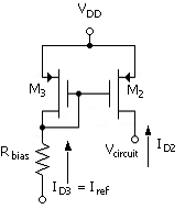
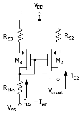
An example of a current source based on PMOS transistors is shown here in Fig. 9.1. It consists of the reference circuit, consisting of transistor M3 and bias resistor Rbias. The reference-circuit transistor is diode connected. The induced VSG3 = VSD3 is applied to the current-source transistor M2. Thus, the drain current, or current-source current of M2 is the mirror of the reference current. In an integrated circuit, any number of current sources can be referenced to the reference current or voltage. Current ratios are implemented with the selection of the relative gate widths of the transistors.
The design of the reference circuit is based on a dc solution to the reference current, ID3. The solution is obtained from the loop equation
Equation 9.1
![]()
and transistor equation
Equation 9.2
![]()
The current in M2 is
Equation 9.3
![]()
where
![]()
and
![]()
W2 and W3 are the transistor gate widths of M2 and M3, respectively, and L is the channel length. In general, the ratio of currents is
Equation 9.4
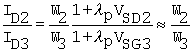
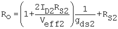
where the approximation can often be used for simplicity with long-channel devices. This avoids the necessity of knowing the source - drain voltages. The signal output resistance at the drain of M2 is
Equation 9.5
![]()
In the project of the current source, we will scan VSD2 and compare the source current with the reference current.
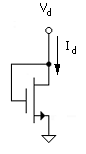
It is normally desirable to have the output resistance of a current source as large as possible. It can be improved over the circuit of Fig. 9.1 by adding resistance in the source branch, as shown in Fig. 9.2, to establish source degeneration (negative feedback). In the discussion of the signal circuit, it is necessary to represent the diode-connected transistor with its linear equivalent, which is just a resistance of magnitude, 1/gm. This can be seen by inspection of the circuit of Fig. 9.3. The voltage, Vd, is applied directly to the gate such that Vgs = Vd and the drain current is Id = gmVd. Thus the resistance of the diode is just Vd/Id = 1/gm. The result is the same for the PMOS and NMOS as is always true for signal linear models.
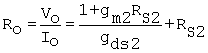
The new output resistance at the drain of M2 for the current-source circuit with source resistors (Fig. 9.2) can be derived based on the signal circuits shown in Fig. 9.4. The output resistance is defined as Ro = Vo/Io, where Io is the drain current flowing in conjunction with the application of the test voltage Vo. Figure 9.4(b) replaces M3 with the signal model equivalent and M2 with the ideal, intrinsic transistor model (current source) along with output resistance,1/gds2. The transistor symbol represents the ideal transistor with output current gm2Vsg2, positive in the direction shown.
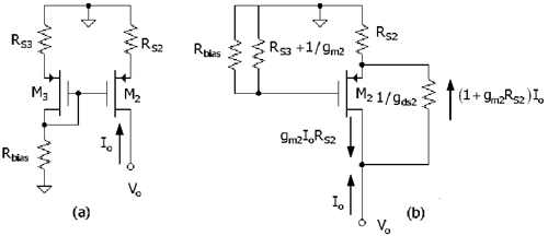
The current Io flowing through the transistor and up through the resistor, RS2, develops a voltage across the resistor, VRS2 = IoRS2. Since Ig2 = 0, an input circuit loop equation is simply Vgs2 = -IdRS2. The transistor linear-model current source, gm2Vgs2, thus is down, as shown in the signal-circuit diagram of Fig. 9.4(b). The sum of currents through 1/gds is
Equation 9.6
![]()
The voltage Vo is thus
Equation 9.7

and the output resistance is
Equation 9.8
This magnitude can be assessed with the use of ( ), which is gm = 2ID/ Veffp. Eliminating gm in (9.8) results in
Equation 9.9
If the magnitude of the voltage across RS2 is several volts, then Ro is much greater than 1/gds2, since Veff2 is typically a fraction of a volt. In integrated circuits, RS may be replaced with an additional current source, in which case the expression becomes
Equation 9.10
![]()
where the output resistance of the added current source is approximately 1/ID2lp
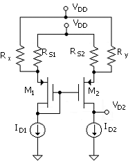
The principle
of the balancing of the differential-amplifier stage (e.g., in an opamp) is
often based on a circuit similar to that in Fig.
9.2,
as shown in Fig.
9.5.
Imbalance could be due, for example, to Vtpo1 ![]() Vtpo2 and kp1
Vtpo2 and kp1 ![]() kp2. Balancing is
implemented by adjusting R1
kp2. Balancing is
implemented by adjusting R1 ![]() R2, where R1 =
RS1//Rx and R2 = RS2||Ry.
R2, where R1 =
RS1//Rx and R2 = RS2||Ry.
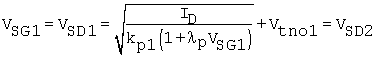
The relationship among the currents, parameters, and resistors is obtained by writing the loop equation around the source resistors and the gate - source terminals, which is
Equation 9.11
![]()
A solution for VSD2 can be obtained from ( ) for a given set of parameters, resistors, and bias variables; on the other hand, Rx and Ry are adjusted to obtain a certain VSD2.
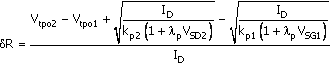
For the special case of ID1 = ID2 = ID, the difference between the resistors in ( ) is
Equation 9.12

For a
numerical example, suppose the goal is to set ![]() By design, in (9.12),
By design, in (9.12),
Equation 9.13
Any slight possible difference in lp is neglected.
In a
practical opamp with this balancing configuration, the source nodes are
connected to external pins. These pins are connected through external resistors
Rx and Ry to VDD as shown in Fig.
9.5.
For adequate adjustment sensitivity, Rx and Ry are
greater than RS1 ![]() RS2 by at least a factor
of 10. In practice, the external resistances are implemented with a
potentiometer.
RS2 by at least a factor
of 10. In practice, the external resistances are implemented with a
potentiometer.
Assume that the transistor parameter values are Vtpo1 = 1.49 V, Vtpo2 = 1.51 V, kp1 = 345 mA/V2, kp2 = 335 mA/V2, and lp = 0.02 V-1. Also assume that the bias current ID = 100 mA. We select RS1 = RS2 = RS = 3 kW (Voltage IDRs = 0.3 V) and we use Rx + Ry = Rpot = 25 kW; the two resistors are segments of a 25-kW potentiometer. The segments of the potentiometer are then determined from a solution to
Equation 9.14
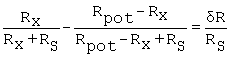
where dR is obtained from ( ) with VSD2 = VSG1 as obtained from ( ). The resistor values are Rx = 16 kW and Ry = 9 kW to give R1 = 2.53 kW and R2 = 2.25 kW
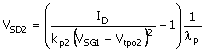
An evaluation of VSD2 without the balancing circuit can be made by setting dR = 0 in ( ) and for solving VSD2 to obtain
Equation 9.15
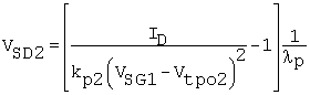
VSG1 is again obtained from (
With the numbers from the example above, VSD2 = 7.87 V. We note that with lp = 0.01 V-1, the solution is VSD2 = 13.2 V and the circuit might well have exceeded the power-supply limits. If Vtpo1 = 1.45 V, Vtpo2 = 1.55 V, and lp = 0.02 V-1 that is, for an extreme case of the difference of threshold voltage, the balancing circuit will still function but now Rx = 21.8 kW and Ry = 3.24 kW with a small R2 = 1.56 kW
|
|
Reference current, ID3, and current-source current, ID2, relation. |
|
|
Output resistance of current-source with source degeneration. |
|
|
Output resistance of current-source with source degeneration and gm = 2ID/Veffp. |
|
|
Relation for setting VD2 in balancing circuit with R1 = RS1//Rx and R2 = RS2 ||Ry. dR = R1 - R2 |
|
|
Relation
for VD2 = VD1 for ID1 |
|
|
VSD2 for unbalanced circuit with dR = 0 and ID1 = ID2 = ID. |
|