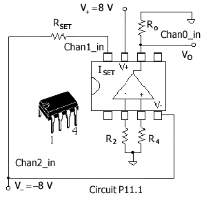
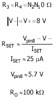
P11.1 SPICE Equations
P11.2 Bias Circuit Setup
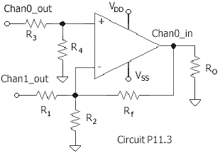
P11.3 Opamp Offset Voltage
P11.4 Evaluation of the Bias Balancing Circuit
P11.5 Evaluation of the Gain and Signal Limits with Swept Input
P11.6 Evaluation of the Gain with Sine-Wave and Square-Wave Signals
P11.7 Determination of the Opamp Frequency Response
Exercises and Analysis Exercise11.mcd - Project11.mcd
|
SPICE Equation |
Description |
|
|
|
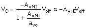
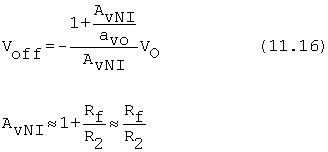
Output voltage of resistance-feedback opamp with offset voltage, Voff. |
|
|
|
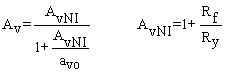
Midfrequency gain dependence on opamp gain avo. |
|
|
|
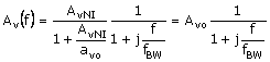
Frequency-response function of resistance-feedback opamp amplifier. |
|
|
|
Bandwidth (corner frequency) of opamp amplifier with opamp open-loop corner frequency, f3dB. |
|
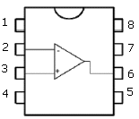
1 Offset Null 1 2 Invert. Input 3 Non-Invert. Input 4 V- 8 ISET 7 V+ 6 Output 5 Offset Null 2
Components
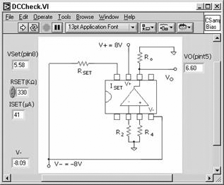
Procedure Do not initially turn on the power supply. Connect the circuit after having made precision measurements of the resistors. Turn on the power supply only with the circuit completely connected, Install the resistor value RSET in the Digital Control of DCCheck.vi. Run the VI. Check the dc values. Verify that ISET is 222v2114c roughly 25mA VO is normally close to V+ or V-. Default and save the Front Panel. |
|
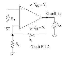
Components Rf
(Very Approximate) AvNI
Procedure Install Rf and re-run DCCheck.vi. Verify that |VO| is less than the value without the feedback resistor. If not, use a smaller Rf.Default and save the information in the Front Panel.
|
||||||||||||||||||||||||
|
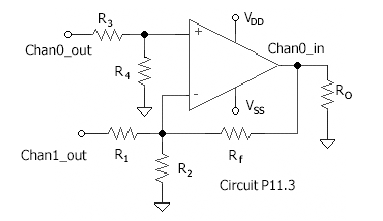
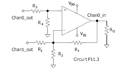
Components R1 = R3 R1/R2 = R3/R4 = 1000 Rf
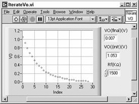
Procedure Connect the additional circuit components, R1 and R3. (Gain measurement results depend on the precision of the values entered.)The VI will sweep Chan1_out to drive the output to near 0 V. Set the value of Rf in the Digital Control of IterateVo.vi.
Run the VI to verify that the balancing circuit is functioning properly. The VI, IterateVo.vi, is a subVI in the amplifier gain evaluations, for balancing the circuit (i.e., for setting the dc output to near 0 V). The indicated VO(init) should match the value from the result of P11.3. Save the Front Panel. |
|
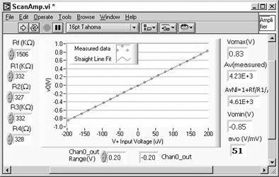
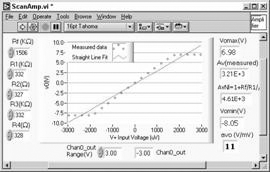
Procedure Enter the resistor values in the Digital Controls of ScanAmp.vi. The gain of interest is amplifier gain, Av = Chan0_in/V+. This is obtained from the measured Slope of n Chan0_in versus Chan0_out and then
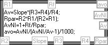
Opamp gain, avo, is calculated in a Formula Node using Av and the ideal gain AvNI = 1 + Rf/R2||R1. Thus, the gain-measurement results depend critically on the precise value of the resistors. Run the VI and reset Chan0_out Range as necessary to obtain an output range of about plus and minus 1 V [graph Y axis and Indicators, Vomax(V) and Vomin(V)]. Save the Front Panel.
Formula Node Computation of avo
Reset the Chan0_out Range, such as in the example (left), to drive the output to the limits. Run the VI and note the limits Vomax(V) (VOH)and Vomin(V)(VOL). Compare these with the datasheet values. Note that the datasheet numbers (below) were obtained for a single power supply and V+ = 10V and V- = 0V. Thus, Vomax approximately 1 V below the power supply and Vomin is approximately 50 m above the negative supply (ground in the datasheet case and -8 V for our opamp amplifier).
|
||||||||||||||||||||||||||||||
|
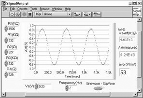
Procedure SignalAmp.vi sends out a sine- or square-wave input signal with a frequency as selected from the Front Panel. Use a frequency of 1 or 2 Hz. It must be low as the frequency response of the amplifier is very low with the high gain of this configuration.
Install resistor values in the Front Panel of SignalAmp.vi.Run the VI and compare the gain for sine- and square-wave signals. Compare for two different frequencies. Adjust Vs for a maximum output signal of about 1 V. Save the Front Panel.
|
||||||||||||||||||||||||||||||
|
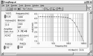
Procedure The VI sweeps the input sine-wave signal over a range of frequencies, 1Hz<f<1kHz. The gain is computed and plotted and the bandwidth of the amplifier is computed and indicated. The GBP is then computed and indicated.
Install precision resistor values for R3 and R4 in the Front Panel of FreqResp.vi. Run the VI to obtain the frequency response. Verify that Vo(max) is less than about 1 V. This must less than the oscilloscope limit of 2 V. Save the Front Panel.
|
||||||||||||||||||
|