Radio
transmitters and receivers have existed since before the end of the nineteenth
century. A practical form of wireless telegraph,
attributed to G. Marconi, appeared in 1895, and successful transmission across
the
In the middle of the twentieth century, the transistor appeared. The idea of transistors based on a sandwich of pn junctions (BJT) and a field-effect transistor based on pn junctions (JFET) and on a metal - oxide - semiconductor (MOS) structure (basically, a capacitor) were all understood at the time. However, pn-junction devices became a practical realization much sooner than the 17217r179r MOS structure, due to fabrication complications in producing the MOS device as well as perhaps a perceived lack of need. The JFET served as an interim field-effect transistor until the MOS technology evolved. It provided for a transistor with very high input resistance and was used extensively as the input transistors for BJT opamps.
A textbook on radio, Elements of Radio, published in 1948 (Marcus and Marcus, 1948), makes no mention of transistors. A 1958 text, (Millman, 1958), Vacuum-Tube and Semiconductor Electronics, gives equal weight to vacuum tubes and BJTs in electronic circuits but makes no mention of the field-effect transistor. Slightly later (Nanavati, 1963), in An Introduction to Semiconductor Electronics, as the title suggests, vacuum tubes are dropped completely and the only reference to a field-effect transistor is in one section of the last chapter and this refers to a junction field-effect transistor. In 1965, in his textbook Analysis and Design of Electronic Circuits, Chirlian devotes a small portion of the book to vacuum tubes, but most of the emphasis is on circuits based on the BJT (Chirlian, 1965). No mention is made of the field-effect-transistor. An example of a book in which BJTs and field-effect transistors of both types were finally given balanced treatment was published in 1979 (Millman, 1979). Textbooks tend to lag the industry a bit, and during the 1970s, MOSFET circuits were emerging rapidly, driven by the simultaneous development of integrated circuits. The four editions of a text on analog circuits by Gray and Meyer, (1977, 1984, 1993) and Gray, et al. (2001) serve well as a series through which we observe a transition from mostly BJT to, in the last two editions, more-or-less equal treatment of BJT and MOSFET devices. A recent textbook on the subject of analog integrated circuits (Johns and Martin, 1997) takes the approach that such circuits are now totally dominated by MOSFETS but includes some BJT applications. BiCMOS, a combination of MOSFET and BJT devices on the same integrated circuit, is growing in popularity as more ways of taking advantage of the superior properties of the two transistor types are developed.
Since the earliest transistors, there has been persistent competition between BJT and MOS transistors. It has been, to a large extent (along with many other considerations), a matter of power consumption versus speed; the BJT has been faster but is associated with high power consumption. The MOSFET has gradually taken over as the most important transistor, with increased emphasis on integrated circuits and improved speeds.
The BJT can be either a pnp or an npn. The MOSFET similarly can be a pmos or an nmos. The equivalents are npn and nmos and pnp and pmos. The following discussion is based on the npn and nmos, as shown in Fig. 2.1. (All polarities and current directions are reversed for the pnp and pmos. This provides for important versatility in applications.)
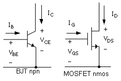
The BJT terminals are designated collector, base, and emitter while those of the MOSFET are drain, gate, and source. The terminal configurations in Fig. 2.1 are, for the BJT, the common emitter, and for the MOSFET, the common source, in amplifier-stage parlance. This suggests that both the input (left side) and output (right side) are referred to the common terminal. For example, for the BJT, the input terminal voltage is VBE and the output terminal voltage is VCE. Similarly, for the MOSFET, we have VGS and VDS. Note that in the convention of subscripts in electronics, the first subscript is assigned positive. This matches the assignments in the diagram, and the plus and minus signs are superfluous.
Note also the convention for symbols for all currents and voltage.
Total voltage and current: vXY, iX
Dc, bias, quiescent, or operating point: VXY, IX
Signal or ac (RMS, peak): Vxy, Ix
General instantaneous signal: vx, ix
The voltage and current symbols in Fig. 2.4 are therefore for dc. For a voltage, a single subscript means that this terminal (or node) voltage is referred to the common terminal. For example, in the npn case above, VCE = VC.
The input terminals vBE and vGS are the control terminals; that is, they control the output currents iC and iD. In both cases, the terminal pairs possess extremely nonsymmetrical voltage - current behavior. With the polarities as shown, the currents flow readily, whereas with the opposite polarities, the output currents are cut off or are, for most purposes, essentially zero.
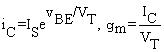
The basic (simplified) general relations between the currents and voltages are:
Equation 2.1
![]()
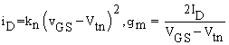
Equation 2.2
![]()
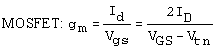
IS, VT, kn, Vtn, and VT are device model parameters or physical constants.
In linear circuit applications, for example, as amplifier stages, the transistors are provided with a circuit configuration that sets up dc, or bias, currents and terminal voltages (sometimes referred to as the Q-point, for quiescent, or in SPICE, the operating point). In the amplifier application, a signal voltage is applied to the input, that is, superimposed on the dc magnitude, which must be much smaller than the dc voltage if the signal input-output relation is to be linear. This is apparent from ( ) and ( ), which are nonlinear relations. All of the currents and terminal voltages will change in response to the input signal, and all of these incremental changes must be small compared to any of the dc currents or voltages, in order for the linear relationships to be valid.
In circuit applications, both types of transistors are operated in all three possible terminal configurations. This provides for a wide variety of amplifier-stage characteristics, including gain and input and output impedance.
The most
fundamental property of a useful electronic voltage amplification device is
that it possess a transconductance that leads
to the possibility of voltage gain. Transconductance is defined as the ratio of the
signal (ac, incremental) current out, iout ![]() diOUT, and the applied input signal voltage, vin
diOUT, and the applied input signal voltage, vin ![]() dvIN. That is, transconductance gm
is
dvIN. That is, transconductance gm
is
Equation 2.3
![]()
For the BJT,
iOUT ![]() iC and vIN
iC and vIN ![]() vBE, while for the NMOS,
iOUT
vBE, while for the NMOS,
iOUT ![]() iD and vIN
iD and vIN ![]() vGS. Thus, ( ) and ( ) can be used for the BJT and
MOSFET, respectively, to obtain an expression for gm. The results
are
vGS. Thus, ( ) and ( ) can be used for the BJT and
MOSFET, respectively, to obtain an expression for gm. The results
are
Equation 2.4
![]()
and
Equation 2.5
IC and ID are the dc (bias) currents of the transistors, so for comparison they can be made equal. At room temperature, the thermal voltage is VT = 26 m. For the MOSFET, VGS is the gate - source bias voltage and Vtn is the transistor threshold voltage. The difference, as in the denominator of the transconductance expression, could typically be about VGS - Vtn = 500 mV.
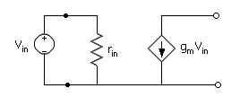
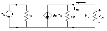
The expression ( ) suggests the linear model given in Fig. 2.2. Included in the model is an input resistance, rin, which accounts for the fact that there can be an incremental current flowing into the input terminal for an increment of input voltage. The model applies in general to amplifying devices, including the vacuum tube (VT), BJT, JFET, and MOSFET. There exists a wide range of magnitude of transconductance and input resistance between the devices. The input resistance, though, affects only the loading of the input signal source; otherwise, the relation of ( ) applies in all cases, and the transconductance is the key to the gain for a given device type. The input resistance is essentially infinite for the vacuum tube and the MOSFET (common source) but can be as low as a few ohms in some configurations for the BJT (e.g., common base).
It is interesting to compare the transconductance of the BJT and MOSFET along with the vacuum tube. We will make a comparison at ID = IC = 10 mA (suitable for a vacuum tube) even though transistors would not usually be operated at such high currents, especially in an integrated circuit. Consulting a source of information for a triode 6SN7 (perhaps one of the most common tubes of all time), one deduces from a graphical analysis the plate characteristics that, for example, gm(VT) = 3 mA/V. From ( ) and ( ), we obtain gm(BJT) = 385 mA/V and gm(MOSFET) = 40 mA/V with VGS - Vtn = 500 mV. The BJT is decidedly superior in this respect, and this is one of the factors contributing to the sustained life of the transistor in industry. That is, the BJT amplifier stage can potentially have a much higher voltage gain. The vacuum tube is clearly inferior to both transistors and points to the reason for the need for so many amplification stages in some VT amplifiers.
The output voltage of amplifiers based on any of the devices will depend on the value of the load resistance, RL, which is added to the circuit of Fig. 2.2 in Fig. 2.3. Note that, in general, RL is not necessarily an actual resistor but could be an effective resistance, as dictated by the amplifier circuitry that is connected to the output of a given stage, combined with a bias resistor. The output voltage induced across RL will be
Equation 2.6
![]()
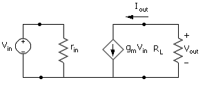
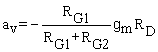
The minus sign is a result of the current flowing up through RL. The signal voltage gain is the incremental output voltage divided by the incremental input voltage such that the gain can readily be obtained from ( ) as
Equation 2.7
![]()
Thus, the gain is directly related to the parameter gm for a given transistor. In general, av can be positive or negative, depending on the terminal configuration. For example, the common base (BJT) and common gate (MOSFET) are positive (noninverting) gain amplifiers.
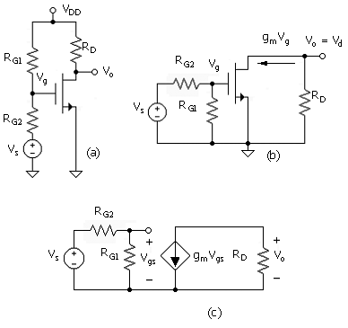
An example of the application of the transconductance relation for the transistor is the basic circuit in Fig. 2.4. Setting dc voltages (in this case, VDD) equal to zero in Fig. 2.4(a) leads to the signal (or ac) circuit [Fig. 2.4(b)]. This follows from the fact that the signal circuit involves only incremental variables (changes) and VDD is a constant.
The schematic symbol for the transistor in the signal circuit associates the output current with the input voltage according to the linear relation of ( ). For linear circuit analysis, the linear equivalent circuit of Fig. 2.2 Fig. 2.4(c)) replaces the linear schematic-symbol representation [Fig. 2.4(b)]. For the MOSFET, rin is infinite and therefore omitted.
The overall gain from the signal source to the output is av = Vo/Vs, which is
Equation 2.8
![]()
where Vo/Vg is ( ) and Vg/Vs is provided by the simple resistor-divider relation given in (
The linear-equivalent circuit of Fig. 2.2 includes an idealization in that the output is a pure current source. In real transistors, the collector (BJT) or drain (MOSFET) current increases with increasing VCE or VDS. This is accounted for by including an output resistance, rout, in the linear model, as added to the circuit in Fig. 2.5. For the BJT and MOSFET, respectively, the value of rout is
Equation 2.9
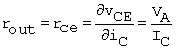
Equation 2.10
![]()
where VA is the characterizing transistor parameter. Note that this voltage dependence is not included in ( ) and ( ); these equations are consistent with the simplified circuit model of Fig. 2.2. Similarly, the voltage dependence will alter gm from the simple forms of ( ) and ( ). This is discussed in Unit 4
The actual gain, with a load RL, which includes the output resistance, can be obtained from modification of ( ) to include rout in parallel with RL as in Fig. 2.5 The result is
Equation 2.11
![]()
The parameter
VA of both transistors can typically be about 100 V. (In MOSFETs,
the parameter is usually referred to as l, which is the
reciprocal, l = 1/VA.) A useful
comparison between the devices is the maximum limiting gain of the
common-emitter and common-source amplifier voltage gains, which applies for the
case of RL ![]()
![]() The gain in
this case is
The gain in
this case is
Equation 2.12
![]()
Using ( ), and ( ), we obtain for the limiting gain:
Equation 2.13
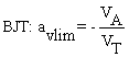
Equation 2.14
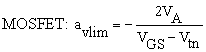
Using sample
numbers from above, the comparison gives av lim(BJT) ![]() -4000 and av lim(MOSFET)
-4000 and av lim(MOSFET) ![]() -400. The vacuum tube, type 6SN7,
has a typical output resistance rout
-400. The vacuum tube, type 6SN7,
has a typical output resistance rout ![]() rp
rp ![]() 7KW (p for plate), which leads to a
limiting gain magnitude of about 21. (This is referred to as the m of the tube.) You have to respect the amplifier designers of the
vacuum-tube era when considering what was accomplished despite the limitations
of these amplifying devices.
7KW (p for plate), which leads to a
limiting gain magnitude of about 21. (This is referred to as the m of the tube.) You have to respect the amplifier designers of the
vacuum-tube era when considering what was accomplished despite the limitations
of these amplifying devices.
In modern integrated circuits, it is possible to implement load circuits, which have an effective RL >> rout such that the limiting gain can be achieved. This is particularly important in MOSFET amplifiers to make up for the relatively low value of gm.
|
|
BJT transfer function and transconductance relation. |
|
|
MOSFET transfer function and transconductance relation. |
|
|
General voltage-gain relation from the transistor input. |
|
|
Gain relation from the signal source. |
|
|
General relation for the transistor output resistance. |
|
|
Voltage gain, including the effect of the transistor output resistance. |
2.6 Exercises and Projects
|
Chirlian, P. M. Analysis and Design of Electronic Circuits.
Gray, P. R., and R. G. Meyer. Analysis and
Design of Analog Integrated Circuits, 1st, 2nd, and 3rd eds. Wiley,
Gray, P. R., P. J. Hurst, S. H. Lewis, and R. G. Meyer. Analysis and Design of Analog Integrated Circuits,
4th ed. Wiley,
Johns, D., and K. Martin. Analog Integrated
Circuits. Wiley,
Marcus, A., and W. Marcus. Elements of Radio,
2nd ed.,
Millman, J. Vacuum-tube and Semiconductor
Electronics.
Millman, J. Microelectronics.
Nanavati, R. P. An Introduction to
Semiconductor Electronics.
|