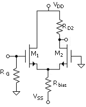
The MOSFET differential amplifier stage is a relatively high-gain stage with grounded dc inputs, which requires no bypass capacitor. The stage also has the important advantage of having two inputs, one inverting and one noninverting. This is essential in operational amplifiers where one or the other (or both) is used, depending on the application. The two inputs also provide for operating the stage in the differential mode, where the input is not referenced to ground. The differential amplifier stage discussed here is an all-resistor circuit with source and drain resistors. In a modern integrated circuit, these are replaced with transistor current sources. However, the principle of operation is the same, and the resistor version can be implemented in our laboratory project.
Various segments of the differential amplifier comprise amplifier stages from all three terminal configurations: the common source, the common gate, and the source follower (common drain). In this unit, a detailed theoretical analysis of all three stages is undertaken (based on Level 1 SPICE). The linear models used include, progressively, the output conductance, gds, and the body-effect transconductance, gmb.
The equation for the dc circuit (Fig. 8.1) is the same as for the current-source common-source stage except that the bias resistor has current 2ID as the current from both transistors is flowing through this resistor. For now, the stage will be assumed to be perfectly balanced such that ID1 = ID2 = ID. The bias equation is
Equation 8.1
Note that the
threshold voltage is that for VSB ![]() 0 V. The solution can be obtained
with the inclusion of the threshold voltage equation, also a function of ID,
0 V. The solution can be obtained
with the inclusion of the threshold voltage equation, also a function of ID,
Equation 8.2
![]()
In the project on the differential amplifier, we can connect the sources and bodies of the two transistors. This is because only NMOS transistors are used in the circuit, and both transistors have the source connected t 14314k1018o o the same node. In this case, Vtn = Vtno.
In a real
transistor, parameters kn, Vtno, and ln can be slightly different such that, in
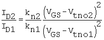
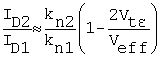
general, ID1 ![]() ID2. The ratio of the currents is given by
ID2. The ratio of the currents is given by
Equation 8.3
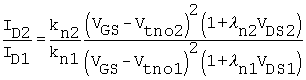
where, in the
circuit with the gate of M1 grounded, VGS1 = VGS2
= VGS. For the specific case of the project on the amplifier, we can
assume that VDS1 ![]() VDS2 such that
VDS2 such that
Equation 8.4
To simplify the relation, it is advantageous to express parameters in terms of increments. For example, threshold voltage will be expressed as a mean value
Equation 8.5
![]()
and a difference between the threshold voltage of the two transistors
Equation 8.6
![]()
such that
Equation 8.7
![]()
and
Equation 8.8
![]()
Using these definitions along with Veff = VGS - Vtno, we have
Equation 8.9
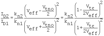
or, approximately,
Equation 8.10
In the
differential amplifier project (PMOS), we measure the drain currents along with
VSG over a range of drain current values. These are used to obtain,
in the Mathcad project file, kn1, kn2, and the threshold
voltages and thus, vt![]() . This will provide a comparison
between the measured drain-current ratios and ( ) as a function of Veff
and drain current.
. This will provide a comparison
between the measured drain-current ratios and ( ) as a function of Veff
and drain current.
This initial assessment of the gain of the differential amplifier neglects the effects of the bias resistor, Rbias, and of the output resistance of the transistors as well as the body effect. These effects are considered below. To generalize the discussion to include the possibility of inverting and noninverting modes of operation, we base the discussion on the circuit (Fig. 8.2) with a drain resistor for both transistors. The inverting and noninverting modes take, respectively, the outputs at Vd1 = Vo1 (av1) and Vd2 = Vo2 (av2). Also, this is the configuration that is studied in the project on the differential amplifier. Note that the input could arbitrarily be moved to the gate of M2, in which case the output taken at Vd1 becomes the noninverting mode, and so forth.
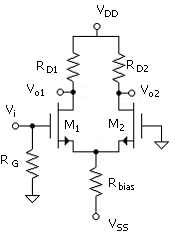
Assume for the present that the amplifier is perfectly symmetrical such that, for example, ID1 = ID2 and gm1 = gm2. A signal voltage Vi is applied to the gate of M1 as shown in the diagram. The voltage divides between the two transistors (from gate 1 to gate 2) to give
Equation 8.11
![]()
Since Vgs1 = |Vsg2| (due to the symmetry of this case), then
Equation 8.12
![]()
The negative Vgs2 results from the fact that the total vGS2 is reduced from bias VGS2 upon the application of a positive signal voltage, Vi, at the gate of M1 (i.e., vGS2 = VGS2 - Vi/2). It follows that total iD2 decreases, which leads to a positive signal voltage at the drain, Vd2. Thus, the amplification is noninverting.
As always, the relation between the signal drain current and the signal drain-source voltage is ( ), which is (with gds = gmb = 0)
Id = gmVgs
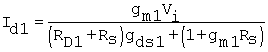
Eliminating Vgs in ( ), applied to M2, with ( ), the drain current for M2 is related to the input voltage, Vi, by
Equation 8.13
![]()
Combining ( ) with Vo2 = -Id2RD2, the output voltage is related to the input voltage by
Equation 8.14
![]()
such that the gain is
Equation 8.15
![]()
Note that there is no minus in the relation; that is, this is the noninverting amplifier mode. Also note that the gain for this amplifier is one-half of that for the common-source amplifier. This is a reasonable price to pay for not having a bypass capacitor. The amplification can be viewed as a source-follower stage in cascade with a common-base stage, neither of which is an inverting stage.
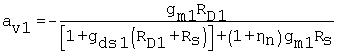
The inverting mode of the amplifier is for the output taken at the drain of M1. For this case, Vo1 = -Id1RD1, and from ( ) and ( ) applied to M1, Id1 = gm1Vg/2 and the voltage relationship is
Equation 8.16
![]()
This leads to the inverting gain, which is
Equation 8.17
![]()
The results above ignore the effect of resistance, Rbias. When it is included, it is no longer valid to assume that Vgs1 = Vsg2, even with ID1 = ID2. The bias-resistor effect is examined here based on a signal equivalent circuit of Fig. 8.3. The resistance at the source of M1 consists of the bias resistor and the linear-model resistance 1/gm2 (which neglects 1/gds2), looking into the source of M2.
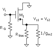
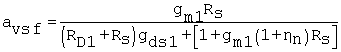
For the noninverting mode, the circuit transconductance, Gm2 = Id2/Vi, is
Equation 8.18
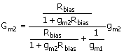
Parameter gm2 is the transconductance Id2/Vs2 (i.e., from the source of M2 to the output Vo2). Note that the fraction is just a voltage divider, Vs2/Vi, since the output resistance at the source of M1 is 1/gm1, as noted in connection with ( ). With gm1 = gm2, the multiplying fraction assumes the value of ½ for very large Rbias.
The noninverting gain, which includes the effect of the bias resistor, is
Equation 8.19
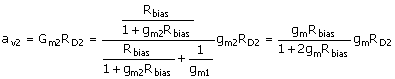
where the right-hand side uses gm1 = gm2. The gain result is technically that of the cascade of a source-follower stage (M1) and a common-gate stage, gm2RD2 (M2). The multiplying fraction is < ½.
The gain for the inverting side can be obtained by using ( ), which is for a common-source amplifier with source resistor. This gives for the inverting-mode gain
Equation 8.20
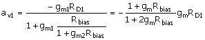
where the right-hand side again uses gm1 = gm2. The multiplying fraction is > ½. Note that for both inverting and noninverting gains, the effect of Rbias can be neglected for most purposes, as the multiplying fractions in ( ) and ( ) are both close to ½.
The choice of the input at gate 1 is arbitrary and all of the results obtained here apply equally to the input taken at gate 2. The inverting output is always at the side of the input, and the noninverting output is always at the opposite side.
Suppose that an input voltage, Vg12 = Vg1 - Vg2, is applied between the inputs. Due to symmetry, the voltage magnitudes at the inputs with respect to ground are Vg1 = Vg12/2 and Vg2 = -Vg12/2, respectively. The noninverting output, Vd2, for this case is, by superposition,
Equation 8.21
![]()
The gains for the contributions from Vg1 and Vg2 are ( ) and ( ), respectively. This is the case of a pure differential input with resulting gain
Equation 8.22
![]()
A similar approach applied to obtain the gain for the output taken as Vd1 produces
Equation 8.23
![]()
Assume, for a numerical example, that ID = 100 mA, RD1 = 50 KW, and gm = 200 mA/V (Veffn = 0.5 V). In this case the gain is avd1 = -10. This would be consistent with VDD = |VSS| = 10 V.
The gain for the case of the differential output, avd12 = (Vd1 - Vd2)/(Vg1 - Vg2), can be obtained from (Vd1 - Vd2) = -(1/2)gm1RD1Vg12 - (1/2)gm2RD2Vg12 and is
Equation 8.24
![]()
where gm1
= gm2 and RD1 = RD2 = RD. Note that
( ) and ( ) are the same as ( ) and ( ). However, ( ) and ( ) are the limiting forms of ( ) and ( ) for Rbias ![]()
![]() , whereas ( ) and ( ) apply for a finite Rbias.
, whereas ( ) and ( ) apply for a finite Rbias.
The common-mode gain is defined for the same voltage applied simultaneously to both inputs. The output must be the same at either output terminal (again assuming that gm1 = gm2 and RD1 = RD2). For example, for the output Vd2, the gain can be determined by a superposition of gains, inverting (input, Vg2) and noninverting (input, Vg1), with RD2 in both equations.
Using ( ) (noninverting) and ( ) (inverting), the gain for finite Rbias is, accordingly,
Equation 8.25
![]()
which is
Equation 8.26
![]()
The result is that of a common-source stage with source resistance 2Rbias. This is intuitively correct as taken from the half-circuit viewpoint, where the circuit is completely symmetrical. The input from either side looks at a common-source stage except that the opposite side is contributing an equal amount of source current, thus giving an effective source resistance equal to twice the actual value. A valid approximate form for well-designed circuits (in terms of common-mode gain) is
Equation 8.27
![]()
The same
result applies to the case of the output taken at the opposite drain, with the
substitution of RD1 for RD2. Using the circuit values
following ( ) plus Rbias = 85 kW, avcm ![]() -0.3. Note that this result in
combination with the gain from ( ) would indicate that this is not a
particularly good design. The goal is for avd >> avcm.
-0.3. Note that this result in
combination with the gain from ( ) would indicate that this is not a
particularly good design. The goal is for avd >> avcm.
In Project 9 we measure the gain of a "balanced" stage with drain resistors for both transistors. The amplifier is the PMOS version of the NMOS amplifier of Fig. 8.2. We obtain an exact Level 1 SPICE solution for the gains for both outputs. The example is used to explore the use of a simulator for obtaining precision results to compare with simple hand calculations.
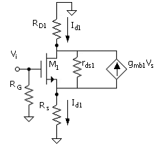
For larger ln values (NMOS), the output resistance can influence the gain and complicate the gain expressions considerably. Here we consider the effect due to gds1 and gds2 while retaining the effect of Rbias. In the following, the gain of the inverting input, av1, is obtained again as a common-source stage with source resistance. The effect of gds2 on the effective source resistance is included (input at the source of M2). The effects due to gds1 are also taken into consideration.
The gain of the noninverting case, av2, is obtained by considering the cascade of the source follower stage (M1) and the common-gate stage (M2), as, in effect, was done in the development of ( ). The source-follower gain takes into account effects from gds1 and gds2, and the gain of the common-gate stage depends on gds2.
The circuit transconductance for a common-source stage with source resistor, with the inclusion of gds, was developed in Unit 4 )]. This will be reviewed and reinforced here in the form of a slightly different approach to the result. The signal circuit for this case is again given in Fig. 8.4. Using the variables of Fig. 8.4, the circuit transconductance is Gm1 = Id1/Vi. The object is thus to obtain a relation between these two variables.
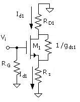
The fraction of the current produced by the intrinsic transistor, gm1Vgs1, which flows into Rs is
Equation 8.28
This is the portion of current source gm1Vgs1, shared between 1/gds and RD + Rs, which flows through RD + Rs, that is, Id1. Note that RD + Rs and 1/gds1 are in parallel and shunt the transistor current source.
A relation for Vgs1 in terms of Id1 follows, which is
Equation 8.29
The input Voltage is the sum of Vgs1 and the drop across Rs. That is,
Equation 8.30
![]()
Using (8.29) in ( ) gives
Equation 8.31
![]()
or
Equation 8.32
The circuit transconductance follows as
Equation 8.33
![]()
The gain for this case is then
Equation 8.34
![]()
A discussion of Rs as affected by gds2 follows.
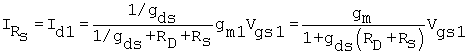
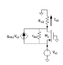
The circuit diagram of Fig. 8.5 is for the M2 portion of the differential amplifier. The input is applied at the source, Vs2, and the output is taken at the drain, Vd2 = Vo2, while the gate is grounded. This is a common-gate configuration. Here we analyze the input resistance, for evaluating the effect on Rs, and gain of the common-gate stage.
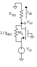
Without gds2, the input resistance at the source is just 1/gm2. With gds2 in place, there is a positive feedback from the drain output to the source input. This causes the input resistance to increase. With gds2, the current into the source terminal is
Equation 8.35
![]()
It is noted that the gds2 term reduces the input current, which has the effect of increasing the input resistance. From ( ), the resulting input resistance at the source, Ris2 = Vs2/Id2, is
Equation 8.36
![]()
The input resistance goes to 1/gm2, as noted above, for gds2 = 0. The expression for the equivalent Rs is now Rs = Rbias || Ris2, where Ris2 is ( ). In modern integrated circuits, RD2 may be replaced with a high-resistance transistor current source, and the input resistance is this case can be much greater than 1/gm2.
The gain of the common-gate stage is obtained as follows: The output voltage is
Equation 8.37
![]()
which gives
Equation 8.38
![]()
Note that for gds2 = 0, the gain has the same magnitude as the simple case for the common-source stage.
The noninverting amplifier gain is based on a cascade of a source-follower stage (M1) and a common-gate stage (M2). The source-follower transconductance, Id1/Vi, is ( ). Using this with Vs1 = Id1Rs gives
Equation 8.39
![]()
Note that the magnitude is about ½. Overall gain is the product of ( ) and ( ), which is
Equation 8.40
![]()
The equations from this unit are summarized below in Unit 8.11
Recall from the discussion of MOSFET model parameters that gds is given by ( ), which is
![]()
Thus, the gain expression depends on parameter l, and especially if l is somewhat large. In Project 9 we measure the gains from the two drains and use the results to find the value of l that makes the theory fit the measurements. In this way, we are getting a signal-derived experimental number to compare with that obtained in the parameter-determination project. This will be done using the PMOS configuration since the value of lp is large and the effect is significant. All of the gain expressions, which are based on NMOS transistors, apply exactly to the PMOS stage with substitution of subscripts; change n to p (parameters) and reverse the order for dc voltage variables.
For hand
calculations, approximate forms must reasonably be used. This applies to
approximate forms for device parameters and gain. The basic gain equations are,
again, assuming that gds = 0 and Rbias = ![]() , simply, as given by ( ) and (
, simply, as given by ( ) and (
![]()
with RD1 = RD2 and gm1 = gm2. In the differential amplifier project, we will compare these with the more precision forms.
In Project 9 we are able to connect the sources of the transistors to the chip body. Certainly, in general this cannot be done such that there is a body effect associated with the differential-amplifier-stage transistors. The necessary alterations to the gain equations are determined in the following. At the end of this unit, we will have the complete, precision-gain calculation equations of Level 1 SPICE. It will be informative to consider numerical results that are based on various degrees of approximations, and this is done below.
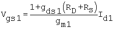
With the body effect present, a component of current, gmb1Vs (Fig. 8.6), is subtracted from gm1Vgs1 such that ( ) for this case is modified to become
Equation 8.41
![]()
Additionally using Vs = Id1Rs and Vgs1 = Vi - Id1Rs ( )] in ( ), a relation between Id1 and Vi is obtained, which is
Equation 8.42
![]()
Solving for Id1, the circuit transconductance is, for the body-effect case,
Equation 8.43
![]()
It follows that the gain for the inverting mode, with the addition of body effect, is
Equation 8.44
The effect of hn in the denominator tends to make the gain smaller. However, the body effect, as shown below, will decrease Rs such that the two effects tend to cancel one another.
The voltage applied to the common-gate stage is Vs2 = Vsg2 (Fig. 8.7). Recall that in the g model for the transistor, as discussed for the common-source mode, current sources gmbVsb and gmVgs are in parallel but in opposite directions. Thus, the current sources gmVsg and gmbVsb are, for the common-gate mode, in the same direction since Vsb = Vsg = -Vgs; the common-gate has an effect transconductance of (1 + h)gm. It follows that the input resistance of the common-gate stage is as obtained before the body effect was included [( )], except for the addition of hn, as in the following:
Equation 8.45
![]()
Similarly, the common-gate gain, ( ), is readily modified with the addition of the multiplying factor (1 + hn This is
Equation 8.46
![]()
Note that in the absence of gds2, the gain for the common-source stage reduces to avcd = gm2 (1 + hn)RD2, where, with body effect, the effective transconductance is, again, (1 + hn) gm2.
The transconductance relation obtained for the common-source stage given by ( ) also applies to the source-follower stage. Combining this with Vs1 = Id1Rs leads to the source-follower gain associated with M1, which is
Equation 8.47
The overall gain is again
av2 = avsf avcg
Note that the body effect for the source-follower stage increases the denominator of ( ) while it increases the numerator in the common-gate result, ( ). These tend to cancel, as in the case of the inverting gain.
For inputs at either or both gates, there exists a common-mode and differential-mode voltage. These are, for applied voltages Vg1 and Vg2, common mode
Equation 8.48
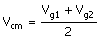
and differential mode
Equation 8.49
![]()
Based on these definitions, the output, for example, Vd1, for a given set of inputs is
Equation 8.50
![]()
where avd1 and avcm are ( ) and ( ) (with RD1), respectively. For the output Vd2, avd2 is substituted for avd1. Vdm is a pure differential input and is not with respect to ground; the effect from the bias resistor is accounted for in the common-mode gain.
For the case of a single-ended input, for example, Vg1 = Vi and Vg2 = 0, the output is
Equation 8.51
![]()
This is identical to ( ). The common-mode contribution can be significant, for example, in a resistance feedback amplifier (Unit 11). In this case, Vdm in ( ) can be very small compared to Vcm.
Gain
calculations were made using kn = 1000 mA/V2, ln = 0.05 V-1, RD = 150 kW, Rbias = 100kW hn = 0.15,
ID = 50 mA, and VDS = 5 V. The
values are given in Table
8.1.
For the comparison, gm was calculated with the precision form [( ln ![]() 0) for all cases. Possibly a more
valid consistency (hand calculation versus precision calculation) would be
achieved with the use of the approximate form for gm up to ln
0) for all cases. Possibly a more
valid consistency (hand calculation versus precision calculation) would be
achieved with the use of the approximate form for gm up to ln ![]() 0. This would reduce some of the
difference in the results. For example, for the first case, av1 = -av2
= -33.5, with the approximate form for gm (ln
0. This would reduce some of the
difference in the results. For example, for the first case, av1 = -av2
= -33.5, with the approximate form for gm (ln ![]()
|
TABLE 8.1 |
||
|
Gain Magnitudes |
av1 |
av2 |
|
Rbias = | ||
|
plus Rbias = 100KW | ||
|
plus ln = 0.05V-1 | ||
|
plus hn | ||
It is notable that the various factors do not have a major effect on the results, even though the value of ln is relatively large. This is especially true for the differential amplifier with resistive load, as considered here. The conclusion can be made that for initial hand-calculation purposes, the simplest form is satisfactory. Precision results can be obtained with a simulator.
|
|
Differential-stage bias equation. |
|
|
Threshold voltage for with VB = VSS and thus VSB = 2IDRbias. |
|
|
Approximate
relation for drain-current imbalance due to kn1 |
|
|
Ideal
voltage gain, Rbias |
|
|
Gain Vd2/Vg1 = Vo2/Vi for noninverting output with finite Rbias. |
|
|
Gain Vd1/Vg1 = Vo1/Vi for inverting output with finite Rbias. |
|
Rs = Ris2 || Rbias |
Gain Vd1/Vg1
= Vo1/Vi for inverting output for source resistance, Rs,
with gds |
|
|
Input at
the source of M2 with gds |
|
|
Gain Vd2/Vs2
= Vo2/Vs2 for common-gate stage of M2 for gds
|
|
|
Gain Vs1/Vg1 = Vs1/Vi of source-follower with input at gate of M1 and output at source of M1. |
|
|
Gain Vd2/Vg1
= Vo2/Vi for noninverting output and gds |
|
avd12 = -gmRD |
Gain for differential input, differential output with RD1 = RD2 and gm1 = gm2. |
|
|
Common-mode gain. |
|
Rs = Ris2 || Rbias |
Inverting-input gain Vd1/Vg1 = Vo1/Vi, including body effect. |
|
|
Input at
the source of M2, including body effect and gds |
|
|
Common-gate gain Vd2/Vs2 = Vo2/Vs2 of M2, including body effect. |
|
|
Source-follower gain Vs1/Vg1 = Vs1/Vi of M1, including body effect. |
|
av2 = avsfavcg |
Gain Vd2/Vg1
= Vo2/Vi, including body effect, gds |
![]()
|
Project Mathcad Files |
Exercise09.mcd - Project09.mcd |
|
Laboratory Project 9 |
MOSFET Differential Amplifier Stage |
|
P9.2 |
DC Evaluation of the Single-Power-Supply Differential Amplifier |
|
P9.3 |
Determination of the PMOS Parameters |
|
P9.4 |
Amplifier Gain Measurement |
|
P9.5 |
Transistor Parameters and DC Imbalance |
|
P9.6 |
Common-Mode Gain Measurement |
|