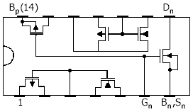
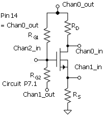
P7.1 SPICE Equations and Pin Diagram
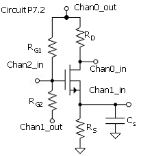
P7.2 NMOS Common-Source Amplifier DC Evaluation
P7.3 Amplifier Gain at Optimum Bias for Linear Output
P7.4 Optimum Bias Stability Test
P7.5 Amplifier Frequency Response
Exercises and Analysis Exercise07.mcd - Project07 1.mcd - Project07 2.mcd
|
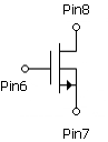
CD4007 Pin Diagram
|
||
|
SPICE Equation |
Description |
|
|
|
(NMOS) |
Dc current - voltage relation. |
|
|
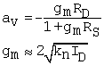
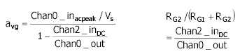
Voltage gain versus ID. |
|
|
|
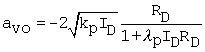
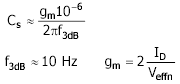
Voltage gain versus ID with bypass capacitor Cs. |
|
|
|
Corner frequency (f3dB) with capacitor Cs. |
|
|
|
Precision fs. |
|
|
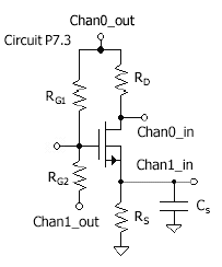
Procedure (Design) Start in the Mathcad fi 616v211g le Project07.mcd to compute circuit component values as follows: We will design for a selected IDmax at Chan0_outmax = 10 V with VDSmin = 1V. Select your IDmax in the range 100 mA < IDmax < 500 mA. Make RG1 = RG2 VG = Chan0_outmax/2. Select the circuit source resistor, RS, to satisfy VG = VGS (IDmax) + IDmaxRs. VGS (IDmax) can be calculated using previously measured parameters or obtained graphically from, for example, NMOSparam.vi from Project 4 After acquiring a real RS (which is close to the calculated value), calculate an actual, new IDmax using the same equation in reverse with the real RS. Neglect the change in VGS. We will select RD to set the condition of VDSmin = 1 V (at Chan0_outmax) from RD = (VDD - VDSmin)/IDmax- Rs. (Use actual, new IDmax.)
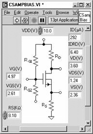
Procedure (Measurement) Install your value of RS in CSAMPBIAS.vi (for current sensing). With VDD = 10 V (VDDmax), run the VI to verify the design. VDSmin can be significantly different from design 1 V due to parameter variation. For example, 1 < VDSmin < 1.5 V is satisfactory, where the low limitation is based on VDSmin > Veffn. This is the requirement to be in the active region. In the example, the design drain current is IDmax = 300 mA. Verify that as VDD is reduced, ID decreases and VDS increases. Check VDD = 4 V, the minimum in the sweep for parameter measurement of the next part. Verify that at the minimum VDD, VDS > ID·RD Obtain a log for Chan0_out = 10V. Reduce VDD from the maximum VDD = 10 V and determine, approximately,
the value between 4V < VDD < 10V that corresponds to VDS
|
|
Components*
Note that gm is in mA/V. Run the first part of Procedure with GainNMOS.vi, below, without the capacitor, to obtain Veffn and bias ID, for computing gm.
LabVIEW Computations Parameters: Vtno, kn
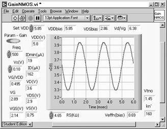
Procedure (Obtain Parameters and Bias Variables) Open GainNMOS.vi. Install your RS value. Without the capacitor installed, set the Mode Switch to Param (red, switch in logic state 0). Run the VI for a VDD sweep to get the parameters. (Note: The sweep rate is configured to be slow in case the capacitor is in place during the sweep.) The VDD sweep is from 4 V to 10 V. Obtain a log of the results. Procedure (Gain Measurement) In the Param mode, the VI finds and indicates VDDbias corresponding to the optimum VDS = (VDD - VRs + Veffn)/2. This permits maximum signal swing without distortion. Set the indicated value of VDDbias into the Set VDD Digital Control. Run the VI with the Mode Switch set to Gain (green, switch position logic 1) without the capacitor. Obtain a log of the Front Panel. Default and save the Front Panel. At the end of the parameter sweep, Veffn is indicated for VDDbias. The value is retained in the Digital Indicator in the gain measurement. The value of ID indicated in the gain measurement is the amplifier gain bias value. Use Veffn along with bias ID, to compute gm and thus Cs. Use Project07.mcd for the calculation. Install the capacitor. Make certain that the polarity of the capacitor is correct. Check that the Mode Switch is set to Gain (switch position logic 1). Check that the value of VDDbias matches the value in Set VDD Digital Control. The VI will measure the gain at this one VDD setting (optimum for distortion-free output). The signal frequency is initially 500 Hz. Run the VI and vary the value of Vs to determine that the gain result, Vd/Vg, is not affected by changes, that is, by distortion. Default and save the Front Panel. Obtain a log of the results. Also, run with slight variations in Freq (e.g., 300 Hz). Note that the parameter values are preserved when running the gain mode. Parameter, bias variable, and gain data are required for the project Mathcad file. |
|
As will be explored in a project Mathcad file, the basis stability computation is performed here with LabVIEW. Recall (Section 5.5) that this takes into consideration a possible range of Vtno and kn values. Here, an analysis is made regarding the extent to which your design is optimum in terms of bias stability. Note that this is separate from the maximum signal condition that has been included in the design.
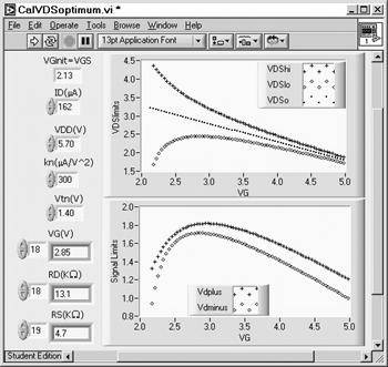
Open CalVDSoptimum.vi. In the Digital Controls, set you values for VDD, kn, Vtno, and ID. ID is the nominal value of the design for the nominal values of the parameters. Your value of ID, along with your parameter values, will be assumed to be, for this evaluation, the nominal values. The computation holds the bias current constant at the design value (as entered into the Front Panel). As VG is increased (X axis), the added increment of VG is the added drop across the new RS, for a given new VG. Run the VI. Verify that the value of VGS in the top Digital Indicator matches reasonably well your measured value (Front Panel of GainNMOS.vi). This SPICE computation uses your measured parameter values and ID. The values should be consistent. The top graph is its VDSlimits versus VG. The center (dashed) curve is
for your parameters. The downward slope reflects the increasing drop across
VG. The top and bottom plots are for the two extremes of VDS that
occur for the worst case of the combination of the limits of kn and Vtno. The computation is for
Vtno± = Vtno ±100 mV and The lower graph contains plots of the output signal limiting values. The best combination of bias stability and signal level is at the peak of these curves. Step through the RS Array Digital Indicator to locate your RS and the associated index. Then determine the corresponding VG and RD (same index). The value of RD should match your design value. The value of VG should match the value from the Front Panel of GainNMOS.vi. Locate your value of VG on the X-axis of the two graphs. If it falls in the range of values surrounding the peaks, the circuit is optimized both in terms of signal limits and bias stability. Note that bias stability was not taken into consideration in the design. In the design, though, often a given criterion serves as the basis and the design may then be evaluated for other criteria. |
|
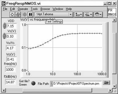
Procedure In FreqRespNMOS.vi, the frequency of the with source voltage (sine-wave Chan1_out) is swept from 1 to 1000 Hz. Chan2_in should be disconnected to reduce the stray capacitance at the gate. In the Front Panel of the VI, set VDDbias and Vs at the values determined in the gain measurement with GainNMOS.vi.
Along with FreqRespNMOS.vi, open FG1Chan.vi to observe the output waveform. Verify that Cs is installed and run the VI to obtain a value for f3dB. Open, from the Diagram of FreqRespNMOS.vi, Frame 2, XYtoDataFile2.vi. Run FreqRespNMOS.vi again, with the data mode switch set to Green (logic stage 1), to obtain a data file of the frequency-response plot in XYtoDataFile2.vi. (Note that with the data VI open, the data are transferred to the VI and can then be saved in the VI.) The data file is used in the Mathcad project file. Default and save the Front Panels of both XYtoDataFile2.vi and FreqRespNMOS.vi. Note the maximum index for the Mathcad file. The f3dB result will differ from the design, as the design was based on the simple form. This will be explored in the Mathcad file. A data file can be obtained later from the saved data in the graph of FreqRespNMOS.vi, with XYtoDataFile2.vi. As noted above, the data file VI can be obtained from the Diagram of FreqRespNMOS.vi. The data file VI is located in Dat.llb in the User.lib folder (Program Files>>National Instruments>>LabVIEW 6). The VI can also be accessed from the menu sequence in FreqRespNMOS.vi, Browse>>Show VI Hierarchy, and open the data file VI from the Hierarchy Window. Return to Project07.mcd. |
|