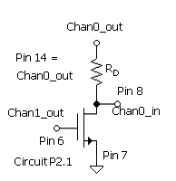
P2.1 NMOS Common-Source Circuit with Drain Current Measurement
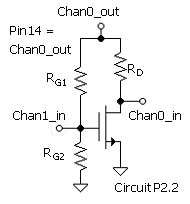
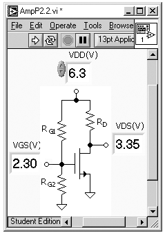
P2.2 NMOS Common-Source Amplifier with Resistor Gate Bias Circuit
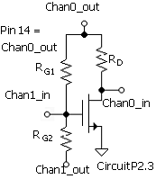
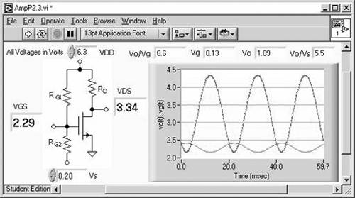
P2.3 Amplifier with Signal and Gain Measurement
Exercises and Analysis Exercise02.mcd - Project02.mcd
|
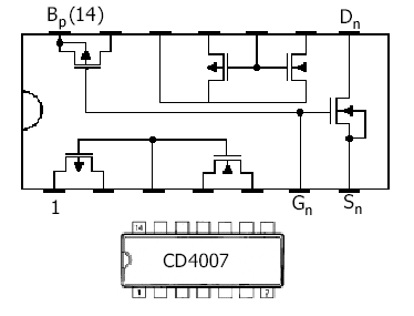
Chip Diagram Connect pin 14 to Chan0_out. Maintain Chan0_out > Chan1_out.
Components
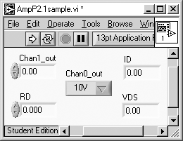
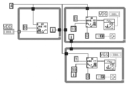
Programming Exercise 2.1 On the Front Panel of a New VI, install two Digital Controls and two Digital Indicators (AmpP2.1.vi). Also install a Menu Ring (Controls>>Ring and Enum>>Menu Ring).
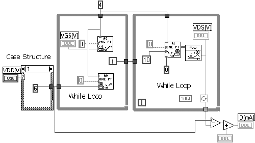
In the Diagram (below), place, from left to right, one Case Structure: Functions>>Structures>>Case, and two While Loops: Functions>>Structures>>While Loop.
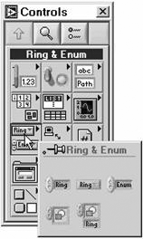
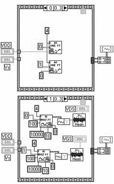
On the Front Panel, using the Text Tool (Shift/Right Click for Tool Palette) in the Menu Ring, type 10 V. Right Click on the Menu Ring and execute Add Item After. In the new listing, type 6 V. Go to the Diagram and wire the output of the Menu Ring to the "?" on the edge of the Case Structure. Note that the Items correspond to integers 0 and 1 at the termi 20220m1211u nal. In the Diagram, place two copies of AO
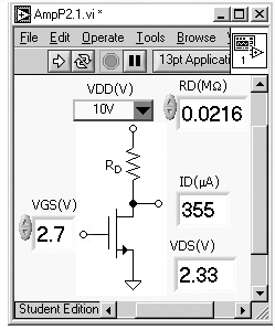
Update Channel.vi in the first (left) While Loop and place AI Sample Channel.vi in the right-hand Install constant values 10 and 6 in the 0 and 1 case states, respectively, and wire to the value terminal of the Chan0_out AO Update Channel.vi icon. Configure the current computation function as in the example (lower-right side in Diagram) and wire to the current Digital Indicator and resistor Digital Control. Optionally, relabel the Digital Controls and Digital Indicators according to their functions (as in AmpP2.1.vi). Procedure Connect the circuit using the RD selected. Install the value of RD(MW) in the Digital Control. To obtain three digits of precision in the resistor Digital Control, Right Click on the Control and go to Format and Precision... Set Digits of Precision. Run AmpP2.1.vi with VDD (Chan0_out) set at 10 V. Adjust VGS (Chan1_out) for a drain voltage, VDS, of roughly 8 to 9 V. Obtain a log of the Front Panel to preserve the current (ID) and VGS information for the Mathcad file. Reminder: Data Logging is under the Operate menu. Now reset VDD to 6 V and re-run. Note that VDS drops by roughly 4 V, indicating that the transistor drain terminal is a current source. Note that the change in the ID indicated is only slight. Reset VDD = 10 V. Increase VGS by an amount that makes VDS about |
P2.2 NMOS Common-Source Amplifier with Resistor Gate Bias Circuit
|
|
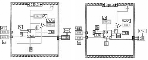
Programming Exercise 2.3 follows below. (Advanced-Optional) Procedure Move the bottom of RG2 from ground to Chan1_out. The VI will send out
a sine-wave signal via this channel with peak Vs. Set Chan0_out (VDD) as in
the circuit for P2.2 above (for VDS Run AmpP2.3.vi (Project02.llb) for various values of Vs. Re-set for a Vo peak of about 1V (VDS/3). Note the gains, which are Vo/Vs and Vo/Vg. Verify that the gain from the source is about two-thirds of the gain the gate, based on the selection (ratio) of the gate bias resistors. Default and save the Front Panel for the Mathcad evaluation.
Programming Exercise 2.3 Make a copy of AmpP2.2.vi with a new name. Go to the Diagram and delete all except Control and Indicator terminals. Install a Sequence Structure in the Diagram (below). In the first Frame, install AO Update Channel.vi. (Functions>>Data Acquisition>>Analog Output.) Press Ctrl and drag (with Arrow Tool) an additional copy, also in Frame 0. Connect a voltage-out (VDD, Chan0_out) value as shown in the example. Connect a numeric 0 (value) to set Chan1_out initially to 0 V for the dc measurements. Connect channel numbers (String) and device number (Numeric, 4 in the example).
Add a Frame After. In this Frame (1), install two copies of AI Acquire Waveform.vi. (in menu Functions>>Data Acquisition>>Analog Input.) These will be used for the dc measurements. A given node voltage will be sampled 100 times and the samples will be averaged for the result. Connect constants to the icons as shown in the example. These include device (Numeric, 4, default), channel (String), number of samples (Numeric, 100), sample rate (Numeric, 10000) high limit (10 V) and low limit (0 V). Place two copies of Get Waveform Components in Frame 1 (Palette Functions>>Waveform>>Get Waveform Components). Then Left Click on the output (right side) of these and select "Y". Connect the inputs to the waveform outputs of AI Acquire Waveform. Connect the outputs of Get Waveform Components to the inputs of Mean.vi functions. These are located in Functions>>Mathematics>>Probability and Statistics or in Functions>>Analyze>>Mathematics>>Probability and Statistics. Connect the outputs of the Mean.vi icons to the terminals of the Digital Indicators of VDS (Chan0_in) and VGS (Chan1_in). Add a Frame After (2). In this Frame we place a general-purpose function generator and oscilloscope function. This is FG1Chan.vi and is in Functions>>User Libraries>>FunctGen. A Digital Control and a Digital Indicator are required for this Frame. Install Digital Control, Vs, and Digital Indicator, Vo.
Connect to FG1Chan.vi, the various terminals, constants, and strings. The connections include Frequency (Numeric, 50), Vacin (Vo), Chan_out (String, 1), Sinewave - SqWave (False), Graph Out (leave disconnected for now), Chan_in (String, 0), Vs (Digital Control), and VDCout (Numeric, 0). Now add another Frame after (3). In this Frame, install the same function, FG1Chan.vi. This can be copied and pasted from Frame 2. Add, in the Front Panel, an additional Digital Indicator, Vg. Make the connections the same as in Frame 2 except Chan_in (String, 1). In Frame 2, configure, using a divide function, Vo/Vs, as shown in the example. Add a Digital Indicator in the Front Panel with the label Vo/Vs and connect the output from the divide function to the terminal of this Digital Indicator. Click on the edge of Frame 2 and install Add Sequence Local and, to this, Connect Vacin (Vo). Move to Frame 3, install a Divide function, and configure Vo/Vg as in the example. Note that Vo comes from the Add Sequence Local from Frame 2. In the Front Panel, add an additional Digital Indicator to read Vo/Vg. Now add the graph in the Front Panel. (A detailed description of using a graph is given in Section A.1.5.) The graph for this case is a Waveform Graph. Get this in the Front Panel under Controls>>Graph>>Waveform Graph. Use the Coloring Tool to adjust the color of the graph background by Right Clicking on the graph with the Coloring Tool. Right Click on the sample trace in the Plot Legend to adjust the color of the trace. Using the Operating Tool, Right Click on the X Scale or Y Scale>>Formatting to set the Grid Options. Configure the Diagram for connecting to the graph. Outside the Sequence Structure and on the right, install a Build Array function. (Functions>>Array>>Build Array.) Connect the Plot output of FG1Chan.vi in the two Frames, 2 and 3, to the two inputs of Build Array. Connect the output of Frame 2 on the top input. |
|